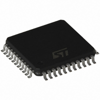
ST72F361J9T6 STMicroelectronics, ST72F361J9T6 Datasheet - Page 161

ST72F361J9T6
Manufacturer Part Number
ST72F361J9T6
Description
IC MCU 8BIT 60K FLASH 44-LQFP
Manufacturer
STMicroelectronics
Series
ST7r
Datasheet
1.ST72F361K6T6.pdf
(225 pages)
Specifications of ST72F361J9T6
Core Processor
ST7
Core Size
8-Bit
Speed
8MHz
Connectivity
LINSCI, SPI
Peripherals
LVD, POR, PWM, WDT
Number Of I /o
32
Program Memory Size
60KB (60K x 8)
Program Memory Type
FLASH
Ram Size
2K x 8
Voltage - Supply (vcc/vdd)
3.8 V ~ 5.5 V
Data Converters
A/D 16x10b
Oscillator Type
External
Operating Temperature
-40°C ~ 85°C
Package / Case
44-LQFP
Processor Series
ST72F3x
Core
ST7
Data Bus Width
8 bit
Data Ram Size
2 KB
Interface Type
LINSCI, SPI
Maximum Clock Frequency
8 MHz
Number Of Programmable I/os
34
Number Of Timers
2
Maximum Operating Temperature
+ 85 C
Mounting Style
SMD/SMT
Development Tools By Supplier
ST72F36X-SK/RAIS, STX-RLINK
Minimum Operating Temperature
- 40 C
On-chip Adc
10 bit, 11 Channel
Lead Free Status / RoHS Status
Lead free / RoHS Compliant
Eeprom Size
-
Lead Free Status / Rohs Status
Details
Available stocks
Company
Part Number
Manufacturer
Quantity
Price
Company:
Part Number:
ST72F361J9T6
Manufacturer:
STMicroelectronics
Quantity:
50
Company:
Part Number:
ST72F361J9T6
Manufacturer:
STMicroelectronics
Quantity:
10 000
LINSCI™ SERIAL COMMUNICATION INTERFACE (LIN Master Only) (Cont’d)
10.8.8 Register Description
STATUS REGISTER (SCISR)
Read Only
Reset Value: 1100 0000 (C0h)
Bit 7 = TDRE Transmit data register empty.
This bit is set by hardware when the content of the
TDR register has been transferred into the shift
register. An interrupt is generated if the TIE bit = 1
in the SCICR2 register. It is cleared by a software
sequence (an access to the SCISR register fol-
lowed by a write to the SCIDR register).
0: Data is not transferred to the shift register
1: Data is transferred to the shift register
Note: Data is not be transferred to the shift register
until the TDRE bit is cleared.
Bit 6 = TC Transmission complete.
This bit is set by hardware when transmission of a
frame containing Data is complete. An interrupt is
generated if TCIE = 1 in the SCICR2 register. It is
cleared by a software sequence (an access to the
SCISR register followed by a write to the SCIDR
register).
0: Transmission is not complete
1: Transmission is complete
Note: TC is not set after the transmission of a Pre-
amble or a Break.
Bit 5 = RDRF Received data ready flag.
This bit is set by hardware when the content of the
RDR register has been transferred to the SCIDR
register. An interrupt is generated if RIE = 1 in the
SCICR2 register. It is cleared by a software se-
quence (an access to the SCISR register followed
by a read to the SCIDR register).
0: Data is not received
1: Received data is ready to be read
Bit 4 = IDLE Idle line detect.
This bit is set by hardware when an Idle Line is de-
tected. An interrupt is generated if the ILIE = 1 in
the SCICR2 register. It is cleared by a software se-
quence (an access to the SCISR register followed
by a read to the SCIDR register).
0: No Idle Line is detected
1: Idle Line is detected
TDRE
7
TC
RDRF
IDLE
OR
NF
FE
PE
0
Note: The IDLE bit is not be set again until the
RDRF bit has been set itself (that is, a new idle line
occurs).
Bit 3 = OR Overrun error.
This bit is set by hardware when the word currently
being received in the shift register is ready to be
transferred into the RDR register while RDRF = 1.
An interrupt is generated if RIE = 1 in the SCICR2
register. It is cleared by a software sequence (an
access to the SCISR register followed by a read to
the SCIDR register).
0: No Overrun error
1: Overrun error is detected
Note: When this bit is set, the RDR register con-
tent is not lost but the shift register is overwritten.
Bit 2 = NF Noise flag.
This bit is set by hardware when noise is detected
on a received frame. It is cleared by a software se-
quence (an access to the SCISR register followed
by a read to the SCIDR register).
0: No noise is detected
1: Noise is detected
Note: This bit does not generate interrupt as it ap-
pears at the same time as the RDRF bit which it-
self generates an interrupt.
Bit 1 = FE Framing error.
This bit is set by hardware when a de-synchroniza-
tion, excessive noise or a break character is de-
tected. It is cleared by a software sequence (an
access to the SCISR register followed by a read to
the SCIDR register).
0: No Framing error is detected
1: Framing error or break character is detected
Note: This bit does not generate an interrupt as it
appears at the same time as the RDRF bit which it-
self generates an interrupt. If the word currently
being transferred causes both frame error and
overrun error, it is transferred and only the OR bit
is set.
Bit 0 = PE Parity error.
This bit is set by hardware when a parity error oc-
curs in receiver mode. It is cleared by a software
sequence (a read to the status register followed by
an access to the SCIDR data register). An inter-
rupt is generated if PIE = 1 in the SCICR1 register.
0: No parity error
1: Parity error
ST72361
161/225


