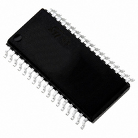
ST72F621L4M1 STMicroelectronics, ST72F621L4M1 Datasheet - Page 113

ST72F621L4M1
Manufacturer Part Number
ST72F621L4M1
Description
IC MCU 8BIT LS 16K 34-SOIC
Manufacturer
STMicroelectronics
Series
ST7r
Datasheet
1.ST72F622L2M1.pdf
(139 pages)
Specifications of ST72F621L4M1
Core Processor
ST7
Core Size
8-Bit
Speed
8MHz
Connectivity
SCI, SPI, USB
Peripherals
DMA, LVD, POR, PWM, WDT
Number Of I /o
23
Program Memory Size
16KB (16K x 8)
Program Memory Type
FLASH
Ram Size
768 x 8
Voltage - Supply (vcc/vdd)
4 V ~ 5.5 V
Data Converters
A/D 8x10b
Oscillator Type
Internal
Operating Temperature
0°C ~ 70°C
Package / Case
34-SOIC (7.5mm Width)
Processor Series
ST72F6x
Core
ST7
Data Bus Width
8 bit
Data Ram Size
768 B
Interface Type
SCI, SPI, USB
Maximum Clock Frequency
12 MHz
Number Of Programmable I/os
23
Number Of Timers
2
Operating Supply Voltage
4 V to 5.5 V
Maximum Operating Temperature
+ 70 C
Mounting Style
SMD/SMT
Minimum Operating Temperature
0 C
On-chip Adc
10 bit
For Use With
497-5046 - KIT TOOL FOR ST7/UPSD/STR7 MCU
Lead Free Status / RoHS Status
Lead free / RoHS Compliant
Eeprom Size
-
Lead Free Status / Rohs Status
In Transition
Other names
497-2112-5
Available stocks
Company
Part Number
Manufacturer
Quantity
Price
Company:
Part Number:
ST72F621L4M1
Manufacturer:
ST
Quantity:
2 272
Company:
Part Number:
ST72F621L4M1
Manufacturer:
ST
Quantity:
5
I/O PORT PIN CHARACTERISTICS (Cont’d)
Figure 71. Typical V
12.9 CONTROL PIN CHARACTERISTICS
12.9.1 Asynchronous RESET Pin
Subject to general operating conditions for V
Notes:
1. Unless otherwise specified, typical data are based on T
2. Data guaranteed by design.
3. Hysteresis voltage between Schmitt trigger switching levels. Based on characterization results, not tested.
4. The I
O ports and control pins) must not exceed I
5. The R
scribed in
6. To guarantee the reset of the device, a minimum pulse has to be applied to RESET pin. All short pulses applied on
RESET pin with a duration below t
t
w(RSTL)out
t
Symbol
h(RSTL)in
R
V
V
V
V
hys
ON
0.09
0.08
0.07
0.06
0.05
0.04
0.03
0.02
0.01
OL
IH
IL
0
IO
ON
current sunk must always respect the absolute maximum rating specified in
Figure
3.5
Schmitt trigger voltage hysteresis
Output low level voltage
(see
Weak pull-up equivalent resistor
Generated reset pulse duration
External reset pulse hold time
pull-up equivalent resistor is based on a resistive transistor (corresponding I
Figure
72). This data is based on characterization results, not tested in production.
Input High Level Voltage
4
Input Low Voltage
DD
73,
Parameter
-V
4.5
Figure
OH
Vdd (V)
vs. V
h(RSTL)in
74)
5
4)
DD
6)
VSS
can be ignored.
(high sink port)
5.5
5)
3)
.
DD
6
V
V
External pin or
internal reset sources
, f
DD
IN
Doc ID 6996 Rev 5
CPU
=
=5V
V
A
Conditions
SS
=25°C and V
, and T
0.25
0.15
0.05
0.2
0.1
I
I
IO
IO
0
=5mA
=2mA
A
3.5
unless otherwise specified.
DD
=5V, not tested in production.
0.7xV
4
Min
V
10
SS
DD
Section 12.2
4.5
Vdd (V)
ON
Typ
400
60
30
6
current characteristics de-
5
1)
and the sum of I
0.3xV
5.5
0.4
Max
V
1
DD
2)
2)
DD
6
1/f
113/139
Unit
SFOSC
mV
kΩ
μs
μs
V
V
V
IO
(I/


