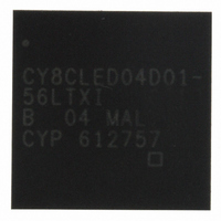
CY8CLED04D01-56LTXI Cypress Semiconductor Corp, CY8CLED04D01-56LTXI Datasheet - Page 18

CY8CLED04D01-56LTXI
Manufacturer Part Number
CY8CLED04D01-56LTXI
Description
IC POWERPSOC 4CH 1A 56VQFN
Manufacturer
Cypress Semiconductor Corp
Series
PowerPSoC® CY8CLEDr
Datasheet
1.CY8CLED03D02-56LTXI.pdf
(47 pages)
Specifications of CY8CLED04D01-56LTXI
Package / Case
56-VQFN Exposed Pad, 56-HVQFN, 56-SQFN, 56-DHVQFN
Core Processor
M8C
Core Size
8-Bit
Speed
24MHz
Connectivity
DALI, DMX512, I²C, IrDA, SPI, UART/USART
Peripherals
LED, LVD, POR, PWM, WDT
Number Of I /o
14
Program Memory Size
16KB (16K x 8)
Program Memory Type
FLASH
Ram Size
1K x 8
Voltage - Supply (vcc/vdd)
4.75 V ~ 5.25 V
Oscillator Type
Internal
Operating Temperature
-40°C ~ 85°C
Operating Supply Voltage
7 V to 32 V
Maximum Supply Current
50 mA
Maximum Operating Temperature
+ 85 C
Mounting Style
SMD/SMT
Minimum Operating Temperature
- 40 C
Lead Free Status / RoHS Status
Lead free / RoHS Compliant
For Use With
428-2882 - KIT STARTER POWERPSOC LIGHTING428-2281 - KIT EVAL POWERPSOC LIGHTING428-2271 - KIT EVAL COLOR-LOCK428-2270 - KIT STARTER DEMO LIGHTING770-1000 - ISP 4PORT FOR CYPRESS PSOC MCU
Eeprom Size
-
Data Converters
-
Lead Free Status / Rohs Status
Lead free / RoHS Compliant
Other names
428-2279
Available stocks
Company
Part Number
Manufacturer
Quantity
Price
Company:
Part Number:
CY8CLED04D01-56LTXI
Manufacturer:
HONEYWELL
Quantity:
1 200
Part Number:
CY8CLED04D01-56LTXI
Manufacturer:
CYPRESS/赛普拉斯
Quantity:
20 000
12.2 CY8CLED04G01 56-Pin Part Pinout (without OCD)
The CY8CLED04G01 PowerPSoC device is available with the following pinout information. Every port pin (labeled with a “P” and
“FN0”) is capable of Digital I/O.
Table 12-2. CY8CLED04G01 56-Pin Part Pinout (QFN)
Document Number: 001-46319 Rev. *E
No.
1
2
3
4
5
6
7
8
9
10
11
12
13
14
15
16
17
18
19
20
21
22
23
24
25
26
27
28
29
30
31
32
33
34
35
36
37
38
39
40
41
42
43
Pin
Digital
Rows
I/O
I/O
I/O
I/O
I/O
I/O
I/O
I/O
I
Columns
Analog
I/O
I/O
Type
I
I
I
I
I
I
Peripherals
Power
O
O
O
O
O
I
I
I
I
I
P1[0]
P2[2]
P0[3]
P0[5]
P0[7]
P1[1]
P1[5]
P1[7]
VSS
NC
NC
NC
NC
XRES
VDD
VSS
AVSS
AVDD
CSN2
CSP2
CSP3
CSN3
SREGCOMP Voltage Regulator Error Amp Comp
SREGFB
SREGCSN
SREGCSP
SREGSW
SREGHVIN
GDVDD
GDVSS
VSS
GD3
NC
VSS
GD2
NC
NC
GD1
VSS
NC
GD0
VSS
GDVSS
Name
GPIO/I2C SDA (secondary), ISSP
primary
GPIO/Direct Switch Cap connection
GPIO/Ainput(coI0) Aoutput (coI0)
GPIO/Ainput(coI0) Aoutput (coI1)
Capsense Ref Cap
GPIO/Connects to Analog Column
Capsense Ref Cap
GPIO/I2C SCLK (secondary) ISSP
primary
GPIO/I2C SDATA (Primary)
GPIO/ I2C SCLK (Primary)
Digital Ground
No Connect
No Connect
No Connect
No Connect
External Reset
Digital Power Supply
Digital Ground
Analog Ground
Analog Power Supply
Current Sense Negative Input 2
Current Sense Positive Input and
Power Supply - CSA2
Current Sense Positive Input and
Power Supply - CSA3
Current Sense Negative Input 3
Regulator Voltage Mode Feedback
Node
Current Mode Feedback Negative
Current Mode Feedback Positive
Switch Mode Regulator OUT
Switch Mode Regulator IN
Gate Driver Power Supply
Gate Driver Ground
Digital Ground
External Low Side Gate Driver 3
No Connect
Digital Ground
External Low Side Gate Driver 2
No Connect
No Connect
External Low Side Gate Driver 1
Digital Ground
No Connect
External Low Side Gate Driver 0
Digital Ground
Gate Driver Ground
Description
Figure 12-2. CY8CLED04G01 56-Pin PowerPSoC Device
Pin
No.
44
45
46
47
48
49
50
51
52
53
54
55
56
Digital
Rows
I/O
I/O
CY8CLED04G01, CY8CLED03G01
CY8CLED04D01, CY8CLED04D02
CY8CLED03D01, CY8CLED03D02
XRES
Columns
P1[0]
P2[2]
P0[3]
P0[5]
P0[7]
P1[1]
P1[5]
P1[7]
VSS
Analog
NC
NC
NC
NC
Type
I
I
1
2
9
11
12
13
14
3
4
5
6
7
8
10
* Connect Exposed Pad to Vss
Peripherals
Power
I/O
I/O
I/O
I/O
I
I
QFN Top View
Exposed
GDVDD Gate Driver Power Supply
FN0[0]
FN0[1]
FN0[2]
FN0[3]
CSN0
CSP0
CSP1
CSN1
P0[4]
VDD
VSS
P1[4]
Pad
Name
Function I/O
Function I/O
Function I/O
Function I/O
Current Sense Negative Input 0
Current Sense Positive Input and
Power Supply - CSA0
Current Sense Positive Input and
Power Supply - CSA1
Current Sense Negative Input 1
GPIO/Connects to Analog Column (1),
connects to bandgap output
Digital Power Supply
Digital Ground
GPIO / External Clock Input
42
35
41
40
39
38
37
36
34
32
31
30
29
33
Description
VSS
GD0
NC
VSS
GD1
NC
NC
GD2
VSS
NC
GD3
VSS
GDVSS
GDVDD
Page 18 of 47
[+] Feedback


