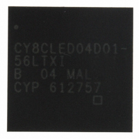
CY8CLED04D01-56LTXI Cypress Semiconductor Corp, CY8CLED04D01-56LTXI Datasheet - Page 31

CY8CLED04D01-56LTXI
Manufacturer Part Number
CY8CLED04D01-56LTXI
Description
IC POWERPSOC 4CH 1A 56VQFN
Manufacturer
Cypress Semiconductor Corp
Series
PowerPSoC® CY8CLEDr
Datasheet
1.CY8CLED03D02-56LTXI.pdf
(47 pages)
Specifications of CY8CLED04D01-56LTXI
Package / Case
56-VQFN Exposed Pad, 56-HVQFN, 56-SQFN, 56-DHVQFN
Core Processor
M8C
Core Size
8-Bit
Speed
24MHz
Connectivity
DALI, DMX512, I²C, IrDA, SPI, UART/USART
Peripherals
LED, LVD, POR, PWM, WDT
Number Of I /o
14
Program Memory Size
16KB (16K x 8)
Program Memory Type
FLASH
Ram Size
1K x 8
Voltage - Supply (vcc/vdd)
4.75 V ~ 5.25 V
Oscillator Type
Internal
Operating Temperature
-40°C ~ 85°C
Operating Supply Voltage
7 V to 32 V
Maximum Supply Current
50 mA
Maximum Operating Temperature
+ 85 C
Mounting Style
SMD/SMT
Minimum Operating Temperature
- 40 C
Lead Free Status / RoHS Status
Lead free / RoHS Compliant
For Use With
428-2882 - KIT STARTER POWERPSOC LIGHTING428-2281 - KIT EVAL POWERPSOC LIGHTING428-2271 - KIT EVAL COLOR-LOCK428-2270 - KIT STARTER DEMO LIGHTING770-1000 - ISP 4PORT FOR CYPRESS PSOC MCU
Eeprom Size
-
Data Converters
-
Lead Free Status / Rohs Status
Lead free / RoHS Compliant
Other names
428-2279
Available stocks
Company
Part Number
Manufacturer
Quantity
Price
Company:
Part Number:
CY8CLED04D01-56LTXI
Manufacturer:
HONEYWELL
Quantity:
1 200
Part Number:
CY8CLED04D01-56LTXI
Manufacturer:
CYPRESS/赛普拉斯
Quantity:
20 000
15.7 Power Peripheral Current Sense Amplifier
The following table lists guaranteed maximum and minimum specifications for the voltage and temperature ranges: 4.75V to 5.25V
and T
Table 15-12. Current Sense Amplifier DC Specifications
Table 15-13. Current Sense Amplifier AC Specifications
Document Number: 001-46319 Rev. *E
V
V
V
I
I
I
PSR
K
V
C
C
t
t
S,CSA
BIASP
BIASN
SETTLE
POWERUP
ICM
ICM(Tolerant)
SENSE
IOS
IN_CSP
IN_CSN
Symbol
Symbol
HV
J
≤ 115
o
C. Typical parameters apply to VDD of 5V and HVDD of 32V at 25°C. These are for design guidance only.
Output Settling Time to 1% of Final Value
Power Up Time to 1% of Final Value
Input Common Mode Voltage Operating
Range
Non Functional Operating Range
Input Differential Voltage Range
Supply Current - CSA
Input Bias Current (+)
Input Bias Current (-)
Power Supply Rejection (CSP pin)
Gain
Input Offset
CSP Input Capacitance
CSN Input Capacitance
Description
Description
Figure 15-3. Comparator Timing Diagram
19.7
Min
Min
7
0
0
–
–
–
–
–
–
–
–
–
Typ
Typ
20
–
–
–
–
–
–
–
–
–
–
–
–
CY8CLED04G01, CY8CLED03G01
CY8CLED04D01, CY8CLED04D02
CY8CLED03D01, CY8CLED03D02
Max
20.3
150
600
Max
-25
32
32
1
1
2
5
2
5
5
Units
Units
V/V
mV
mA
mV
μA
μA
dB
pF
pF
μs
μs
V
Either terminal of the amplifier must
not exceed this range for functionality
Absolute Maximum Rating for V
should never be exceeded. See
Absolute Maximum Ratings
25
Enabling CSA causes an incremental
draw of 1 mA on the AVDD rail.
f
V
V
SW
SENSE
SENSE
< 2 MHz
= 50 mV to 130 mV
= 50 mV to 130 mV
Notes
Notes
Page 31 of 47
on page
SENSE
[+] Feedback


