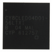
CY8CLED04D01-56LTXI Cypress Semiconductor Corp, CY8CLED04D01-56LTXI Datasheet - Page 44

CY8CLED04D01-56LTXI
Manufacturer Part Number
CY8CLED04D01-56LTXI
Description
IC POWERPSOC 4CH 1A 56VQFN
Manufacturer
Cypress Semiconductor Corp
Series
PowerPSoC® CY8CLEDr
Datasheet
1.CY8CLED03D02-56LTXI.pdf
(47 pages)
Specifications of CY8CLED04D01-56LTXI
Package / Case
56-VQFN Exposed Pad, 56-HVQFN, 56-SQFN, 56-DHVQFN
Core Processor
M8C
Core Size
8-Bit
Speed
24MHz
Connectivity
DALI, DMX512, I²C, IrDA, SPI, UART/USART
Peripherals
LED, LVD, POR, PWM, WDT
Number Of I /o
14
Program Memory Size
16KB (16K x 8)
Program Memory Type
FLASH
Ram Size
1K x 8
Voltage - Supply (vcc/vdd)
4.75 V ~ 5.25 V
Oscillator Type
Internal
Operating Temperature
-40°C ~ 85°C
Operating Supply Voltage
7 V to 32 V
Maximum Supply Current
50 mA
Maximum Operating Temperature
+ 85 C
Mounting Style
SMD/SMT
Minimum Operating Temperature
- 40 C
Lead Free Status / RoHS Status
Lead free / RoHS Compliant
For Use With
428-2882 - KIT STARTER POWERPSOC LIGHTING428-2281 - KIT EVAL POWERPSOC LIGHTING428-2271 - KIT EVAL COLOR-LOCK428-2270 - KIT STARTER DEMO LIGHTING770-1000 - ISP 4PORT FOR CYPRESS PSOC MCU
Eeprom Size
-
Data Converters
-
Lead Free Status / Rohs Status
Lead free / RoHS Compliant
Other names
428-2279
Available stocks
Company
Part Number
Manufacturer
Quantity
Price
Company:
Part Number:
CY8CLED04D01-56LTXI
Manufacturer:
HONEYWELL
Quantity:
1 200
Part Number:
CY8CLED04D01-56LTXI
Manufacturer:
CYPRESS/赛普拉斯
Quantity:
20 000
15.20 PSoC Core I
The following table lists guaranteed maximum and minimum specifications for the voltage and temperature ranges: 4.75V to 5.25V
and T
Table 15-35. AC Characteristics of the I
Document Number: 001-46319 Rev. *E
Note
f
t
t
t
t
t
t
t
t
t
SCLI2C
HDSTAI2C
LOWI2C
HIGHI2C
SUSTAI2C
HDDATI2C
SUDATI2C
SUSTOI2C
BUFI2C
SPI2C
8. A fast mode I2C bus device can be used in a standard mode I2C bus system, but the requirement t
Symbol
if the device does not stretch the LOW period of the SCL signal. If such device does stretch the LOW period of the SCL signal, it must output the next data bit to the
SDA line trmax + t
J
≤ 115°C. Typical parameters apply to 5V at 25°C. These are for design guidance only.
SCL Clock Frequency
Hold Time (repeated) START Condition. After
this period, the first clock pulse is generated.
LOW Period of the SCL Clock
HIGH Period of the SCL Clock
Setup Time for a Repeated START Condition
Data Hold Time
Data Setup Time
Setup Time for STOP Condition
Bus Free Time Between a STOP and START
Condition
Pulse Width of Spikes are Suppressed by the
Input Filter.
SUDATI2
2
C Specifications
= 1000 + 250 = 1250 ns (according to the standard mode I2C bus specification) before the SCL line is released.
Figure 15-8. Definition of Timing for Fast/Standard Mode on the I
Description
2
C SDA and SCL Pins
Standard Mode
Min
250
4.0
4.7
4.0
4.7
4.0
4.7
0
0
–
Max
100
–
–
–
–
–
–
–
–
–
CY8CLED04G01, CY8CLED03G01
CY8CLED04D01, CY8CLED04D02
CY8CLED03D01, CY8CLED03D02
100
SUDATI2
Min
0.6
1.3
0.6
0.6
0.6
1.3
Fast Mode
0
0
0
[8]
≥ 250 ns must then be met. This is automatically the case
Max
400
50
–
–
–
–
–
–
–
–
2
C Bus
Units
kHz
μs
μs
μs
μs
μs
ns
μs
μs
ns
Notes
Page 44 of 47
[+] Feedback


