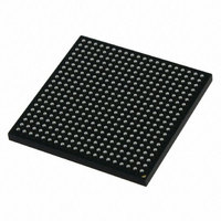
MCIMX251AJM4 Freescale Semiconductor, MCIMX251AJM4 Datasheet - Page 108

MCIMX251AJM4
Manufacturer Part Number
MCIMX251AJM4
Description
IC MPU IMX25 AUTO 400MAPBGA
Manufacturer
Freescale Semiconductor
Series
i.MX25r
Datasheet
1.MCIMX255AJM4.pdf
(140 pages)
Specifications of MCIMX251AJM4
Core Processor
ARM9
Core Size
32-Bit
Speed
400MHz
Connectivity
1-Wire, CAN, EBI/EMI, Ethernet, I²C, MMC, SmartCard, SPI, SSI, UART/USART, USB OTG
Peripherals
DMA, I²S, POR, PWM, WDT
Number Of I /o
128
Program Memory Type
External Program Memory
Ram Size
144K x 8
Voltage - Supply (vcc/vdd)
1.15 V ~ 1.52 V
Data Converters
A/D 3x12b
Oscillator Type
External
Operating Temperature
-40°C ~ 85°C
Package / Case
400-MAPBGA
Lead Free Status / RoHS Status
Lead free / RoHS Compliant
Eeprom Size
-
Program Memory Size
-
Available stocks
Company
Part Number
Manufacturer
Quantity
Price
Company:
Part Number:
MCIMX251AJM4
Manufacturer:
Freescale Semiconductor
Quantity:
10 000
Company:
Part Number:
MCIMX251AJM4A
Manufacturer:
IDT
Quantity:
450
Company:
Part Number:
MCIMX251AJM4A
Manufacturer:
Freescale Semiconductor
Quantity:
135
Company:
Part Number:
MCIMX251AJM4A
Manufacturer:
FREESCALE
Quantity:
648
Company:
Part Number:
MCIMX251AJM4A
Manufacturer:
Freescale Semiconductor
Quantity:
10 000
Part Number:
MCIMX251AJM4A
Manufacturer:
FREESCALE
Quantity:
20 000
Note:
3.7.17.3
Figure 80
parameters (SS22-SS46) shown in the figure.
108
• All the timings for the SSI are given for a non-inverted serial clock polarity (TSCKP/RSCKP = 0) and a non-inverted frame sync
• All timings are on pads when SSI is being used for a data transfer.
• ”Tx” and “Rx” refer to the transmit and receive sections of the SSI.
• For internal frame sync operation using external clock, the FS timing is the same as that of Tx Data (for example, during AC97
(TFSI/RFSI = 0). If the polarity of the clock and/or the frame sync have been inverted, all the timing remains valid by inverting
the clock signal STCK/SRCK and/or the frame sync STFS/SRFS shown in the tables and in the figures.
mode of operation).
SS48
SS49
SS50
SS51
ID
shows the timing for the SSI transmitter with external clock.
Oversampling clock high period
Oversampling clock rise time
Oversampling clock low period
Oversampling clock fall time
Note: SRXD Input in Synchronous mode only
AUDn_TXFS (wl)
SSI Transmitter Timing with External Clock
AUDn_TXFS (bl)
AUDn_RXD
AUDn_TXC
AUDn_TXD
(Output)
(Input)
(Input)
(Input)
(Input)
Figure 80. SSI Transmitter with External Clock Timing Diagram
Table 82. SSI Receiver Timing with Internal Clock (continued)
i.MX25 Applications Processor for Automotive Products, Rev. 8
SS23
Parameter
SS27
SS22
SS37
SS31
SS44
SS26
SS25
SS38
SS45
SS29
Min.
6.0
6.0
—
—
Table 83
SS24
SS33
SS46
describes the timing
SS39
Freescale Semiconductor
Max.
3.0
3.0
—
—
Unit
ns
ns
ns
ns


