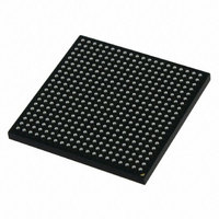
MCIMX251AJM4 Freescale Semiconductor, MCIMX251AJM4 Datasheet - Page 43

MCIMX251AJM4
Manufacturer Part Number
MCIMX251AJM4
Description
IC MPU IMX25 AUTO 400MAPBGA
Manufacturer
Freescale Semiconductor
Series
i.MX25r
Datasheet
1.MCIMX255AJM4.pdf
(140 pages)
Specifications of MCIMX251AJM4
Core Processor
ARM9
Core Size
32-Bit
Speed
400MHz
Connectivity
1-Wire, CAN, EBI/EMI, Ethernet, I²C, MMC, SmartCard, SPI, SSI, UART/USART, USB OTG
Peripherals
DMA, I²S, POR, PWM, WDT
Number Of I /o
128
Program Memory Type
External Program Memory
Ram Size
144K x 8
Voltage - Supply (vcc/vdd)
1.15 V ~ 1.52 V
Data Converters
A/D 3x12b
Oscillator Type
External
Operating Temperature
-40°C ~ 85°C
Package / Case
400-MAPBGA
Lead Free Status / RoHS Status
Lead free / RoHS Compliant
Eeprom Size
-
Program Memory Size
-
Available stocks
Company
Part Number
Manufacturer
Quantity
Price
Company:
Part Number:
MCIMX251AJM4
Manufacturer:
Freescale Semiconductor
Quantity:
10 000
Company:
Part Number:
MCIMX251AJM4A
Manufacturer:
IDT
Quantity:
450
Company:
Part Number:
MCIMX251AJM4A
Manufacturer:
Freescale Semiconductor
Quantity:
135
Company:
Part Number:
MCIMX251AJM4A
Manufacturer:
FREESCALE
Quantity:
648
Company:
Part Number:
MCIMX251AJM4A
Manufacturer:
Freescale Semiconductor
Quantity:
10 000
Part Number:
MCIMX251AJM4A
Manufacturer:
FREESCALE
Quantity:
20 000
Table 32
Figure 8
are shown in the figure.
Figure 9
parameters (OW7–OW8) that are shown in the figure.
Freescale Semiconductor
OW5
OW6
OW1
OW2
OW3
OW4
ID
ID
shows write 0 sequence timing, and
and
lists the RPP timing parameters.
Write 0 Low Time
Transmission Time Slot
Figure 10
1-Wire bus
(OWIRE_LINE)
1-Wire bus
(OWIRE_LINE)
Table 32. RPP Sequence Delay Comparisons Timing Parameters
Presence Detect High
Presence Detect Low
Reset Time High
show write 1 and read sequence timing, respectively.
Reset Time Low
i.MX25 Applications Processor for Automotive Products, Rev. 8
Parameters
Parameter
Table 33. WR0 Sequence Timing Parameters
Figure 8. Write 0 Sequence Timing Diagram
Figure 9. Write 1 Sequence Timing Diagram
OW7
Table 33
OW5
Symbol
t
Symbol
describes the timing parameters (OW5–OW6) that
WR0_low
t
t
t
t
t
RSTH
RSTL
SLOT
PDH
PDL
OW8
OW6
Min.
480
480
OW5
Min.
15
60
60
Table 34
Typ.
511
512
—
—
Typ.
100
117
describes the timing
Max.
240
Max.
60
—
—
120
120
Units
Units
us
us
us
us
μs
μs
43


