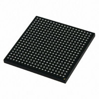
MCIMX251AJM4 Freescale Semiconductor, MCIMX251AJM4 Datasheet - Page 23

MCIMX251AJM4
Manufacturer Part Number
MCIMX251AJM4
Description
IC MPU IMX25 AUTO 400MAPBGA
Manufacturer
Freescale Semiconductor
Series
i.MX25r
Datasheet
1.MCIMX255AJM4.pdf
(140 pages)
Specifications of MCIMX251AJM4
Core Processor
ARM9
Core Size
32-Bit
Speed
400MHz
Connectivity
1-Wire, CAN, EBI/EMI, Ethernet, I²C, MMC, SmartCard, SPI, SSI, UART/USART, USB OTG
Peripherals
DMA, I²S, POR, PWM, WDT
Number Of I /o
128
Program Memory Type
External Program Memory
Ram Size
144K x 8
Voltage - Supply (vcc/vdd)
1.15 V ~ 1.52 V
Data Converters
A/D 3x12b
Oscillator Type
External
Operating Temperature
-40°C ~ 85°C
Package / Case
400-MAPBGA
Lead Free Status / RoHS Status
Lead free / RoHS Compliant
Eeprom Size
-
Program Memory Size
-
Available stocks
Company
Part Number
Manufacturer
Quantity
Price
Company:
Part Number:
MCIMX251AJM4
Manufacturer:
Freescale Semiconductor
Quantity:
10 000
Company:
Part Number:
MCIMX251AJM4A
Manufacturer:
IDT
Quantity:
450
Company:
Part Number:
MCIMX251AJM4A
Manufacturer:
Freescale Semiconductor
Quantity:
135
Company:
Part Number:
MCIMX251AJM4A
Manufacturer:
FREESCALE
Quantity:
648
Company:
Part Number:
MCIMX251AJM4A
Manufacturer:
Freescale Semiconductor
Quantity:
10 000
Part Number:
MCIMX251AJM4A
Manufacturer:
FREESCALE
Quantity:
20 000
Note:
1. OVDD = 1.7 V; V
2. OVDD = 1.7 V; V
3. Vin(dc) specifies the allowable DC excursion of each differential input
4. Vid(dc) specifies the input differential voltage required for switching. The minimum value is equal to Vih(dc) - Vil(dc).
5. Vtt is expected to track OVDD/2.
6. Minimum condition: BCS model, 1.95 V, and –40 °C. Typical condition: typical model, 1.8 V, and 25 °C. Maximum condition:
7. Typical condition: typical model, 1.8 V, and 25 °C. Maximum condition: BCS model, 1.95 V, and 105 °C.
8. The JEDEC SSTL_18 specification (JESD8-15a) for a SSTL interface for class II operation supersedes any specification in
3.5.2
Table 20
Freescale Semiconductor
High-level output voltage
Low-level output voltage
High-level output current for slow
mode
High-level output current for fast
mode
DC input signal voltage(for
differential signal)
DC differential input voltage
Termination voltage
Input current (no pull-up/down)
High-impedance I/O supply
current
High-impedance core supply
current
for parameters V
wcs model, 1.65 V, and 105 °C.
this document.
DC Electrical Characteristics
DC Electrical Characteristics
shows the I/O parameters for GPIO.
GPIO I/O DC Parameters
out
oh
out
Table 19. DDR2 (SSTL_18) I/O DC Electrical Characteristics (continued)
and V
= 280 mV. V
= 1.42 V. (V
ol
for I/O cells is below
i.MX25 Applications Processor for Automotive Products, Rev. 8
out
out
Icc-ovdd VI = OVDD or 0
Symbol
Icc-vddi
-OVDD)/IOH must be less than 21 W for values of V
/IOL must be less than 21 W for values of V
Vin(dc)
Vid(dc)
Table 20. GPIO DC Electrical Characteristics
Symbol
Vtt
IIN
Voh
Ioh
Ioh
Vol
I
I
VI = VDD or 0
Conditions
VI = OVDD
Ioh = Specified Drive
Iol=Specified Drive
Voh=0.8 × OVDD
Voh=0.8 × OVDD
VI = 0
Test Conditions
Test
Standard Drive
Standard Drive
—
—
—
Max. Drive
Max. Drive
Ioh=–1mA
High Drive
High Drive
Iol=1mA
OVDD/2 – 0.04 OVDD/2 OVDD/2 + 0.04
Min.
–0.3
0.25
—
—
—
OVDD – 0.15
0.8 × OVDD
Min.
–2.0
–4.0
–8.0
–4.0
–6.0
–8.0
—
out
between 0 V and 280 mV. Simulation circuit
Typ.
—
—
—
—
—
out
Typ.
—
—
—
—
between OVDD and OVDD-0.28 V.
OVDD + 0.3
OVDD+0.6
0.2 × OVDD
Max.
1210
110
980
60
Max.
0.15
—
—
—
Units
Units Notes
nA
nA
nA
V
V
mA
mA
V
V
Notes
3
4
5
9
9
—
—
1
1
23


