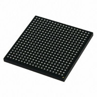
MCIMX251AJM4 Freescale Semiconductor, MCIMX251AJM4 Datasheet - Page 86

MCIMX251AJM4
Manufacturer Part Number
MCIMX251AJM4
Description
IC MPU IMX25 AUTO 400MAPBGA
Manufacturer
Freescale Semiconductor
Series
i.MX25r
Datasheet
1.MCIMX255AJM4.pdf
(140 pages)
Specifications of MCIMX251AJM4
Core Processor
ARM9
Core Size
32-Bit
Speed
400MHz
Connectivity
1-Wire, CAN, EBI/EMI, Ethernet, I²C, MMC, SmartCard, SPI, SSI, UART/USART, USB OTG
Peripherals
DMA, I²S, POR, PWM, WDT
Number Of I /o
128
Program Memory Type
External Program Memory
Ram Size
144K x 8
Voltage - Supply (vcc/vdd)
1.15 V ~ 1.52 V
Data Converters
A/D 3x12b
Oscillator Type
External
Operating Temperature
-40°C ~ 85°C
Package / Case
400-MAPBGA
Lead Free Status / RoHS Status
Lead free / RoHS Compliant
Eeprom Size
-
Program Memory Size
-
Available stocks
Company
Part Number
Manufacturer
Quantity
Price
Company:
Part Number:
MCIMX251AJM4
Manufacturer:
Freescale Semiconductor
Quantity:
10 000
Company:
Part Number:
MCIMX251AJM4A
Manufacturer:
IDT
Quantity:
450
Company:
Part Number:
MCIMX251AJM4A
Manufacturer:
Freescale Semiconductor
Quantity:
135
Company:
Part Number:
MCIMX251AJM4A
Manufacturer:
FREESCALE
Quantity:
648
Company:
Part Number:
MCIMX251AJM4A
Manufacturer:
Freescale Semiconductor
Quantity:
10 000
Part Number:
MCIMX251AJM4A
Manufacturer:
FREESCALE
Quantity:
20 000
3.7.9
The FEC is designed to support both 10- and 100-Mbps Ethernet networks compliant with the IEEE 802.3
standard. An external transceiver interface and transceiver function are required to complete the interface
to the media. The FEC supports 10/100 Mbps MII (18 pins altogether), 10/100 Mbps RMII (ten pins,
including serial management interface) and the 10-Mbps-only 7-Wire interface (which uses seven of the
MII pins), for connection to an external Ethernet transceiver. All signals are compatible with transceivers
operating at a voltage of 3.3 V.
The following subsections describe the timing for MII and RMII modes.
3.7.9.1
The following subsections describe MII receive, transmit, asynchronous inputs, and serial management
signal timings.
3.7.9.1.4
The receiver functions correctly up to an FEC_RX_CLK maximum frequency of 25 MHz + 1%. There is
no minimum frequency requirement. Additionally, the processor clock frequency must exceed twice the
FEC_RX_CLK frequency.
Figure 55
the figure.
1
86
M1
M2
M3
M4
FEC_RX_DV, FEC_RX_CLK, and FEC_RXD0 have the same timing in 10 Mbps 7-wire interface mode.
ID
FEC_RXD[3:0] (inputs)
FEC_RX_CLK (input)
FEC_RXD[3:0], FEC_RX_DV, FEC_RX_ER to FEC_RX_CLK setup
FEC_RX_CLK to FEC_RXD[3:0], FEC_RX_DV, FEC_RX_ER hold
FEC_RX_CLK pulse width high
FEC_RX_CLK pulse width low
shows MII receive signal timings.
Fast Ethernet Controller (FEC) Timing
FEC MII Mode Timing
FEC_RX_DV
FEC_RX_ER
MII Receive Signal Timing (FEC_RXD[3:0], FEC_RX_DV, FEC_RX_ER, and
FEC_RX_CLK)
i.MX25 Applications Processor for Automotive Products, Rev. 8
Figure 55. MII Receive Signal Timing Diagram
Characteristic
Table 62. MII Receive Signal Timing
M1
1
Table 62
M2
M3
describes the timing parameters (M1–M4) shown in
Min.
35%
35%
5
5
M4
Max.
65%
65%
—
—
Freescale Semiconductor
FEC_RX_CLK period
FEC_RX_CLK period
Unit
ns
ns


