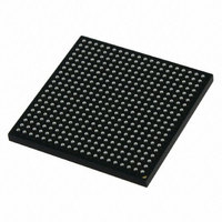
MCIMX251AJM4 Freescale Semiconductor, MCIMX251AJM4 Datasheet - Page 112

MCIMX251AJM4
Manufacturer Part Number
MCIMX251AJM4
Description
IC MPU IMX25 AUTO 400MAPBGA
Manufacturer
Freescale Semiconductor
Series
i.MX25r
Datasheet
1.MCIMX255AJM4.pdf
(140 pages)
Specifications of MCIMX251AJM4
Core Processor
ARM9
Core Size
32-Bit
Speed
400MHz
Connectivity
1-Wire, CAN, EBI/EMI, Ethernet, I²C, MMC, SmartCard, SPI, SSI, UART/USART, USB OTG
Peripherals
DMA, I²S, POR, PWM, WDT
Number Of I /o
128
Program Memory Type
External Program Memory
Ram Size
144K x 8
Voltage - Supply (vcc/vdd)
1.15 V ~ 1.52 V
Data Converters
A/D 3x12b
Oscillator Type
External
Operating Temperature
-40°C ~ 85°C
Package / Case
400-MAPBGA
Lead Free Status / RoHS Status
Lead free / RoHS Compliant
Eeprom Size
-
Program Memory Size
-
Available stocks
Company
Part Number
Manufacturer
Quantity
Price
Company:
Part Number:
MCIMX251AJM4
Manufacturer:
Freescale Semiconductor
Quantity:
10 000
Company:
Part Number:
MCIMX251AJM4A
Manufacturer:
IDT
Quantity:
450
Company:
Part Number:
MCIMX251AJM4A
Manufacturer:
Freescale Semiconductor
Quantity:
135
Company:
Part Number:
MCIMX251AJM4A
Manufacturer:
FREESCALE
Quantity:
648
Company:
Part Number:
MCIMX251AJM4A
Manufacturer:
Freescale Semiconductor
Quantity:
10 000
Part Number:
MCIMX251AJM4A
Manufacturer:
FREESCALE
Quantity:
20 000
1
2
3
4
3.7.18.2
Figure 82
of the internal ADC. After a conversion cycle eoc is asserted, a new conversion begins only when the
112
Current consumption
NVCC_ADC
QV
Power-down current
NVCC_ADC
QV
Expected plate resistance
Switch drivers on
resistance
DNL
INL
Gain + Offset Error
This comprises only the required initial dummy conversion cycle. Additional power-up time depends on the enadc , reset and
soc signals applied to the touchscreen controller.
This value only includes the ADC and the driver switches, but it does not take into account the current consumption in the
touchscreen plate. For example, if the plate resistance is 100 W, the total current consumption is about 33 mA.
At avdd = 3.3 V, dvdd = 1.2 V, Tjunction = 50 °C, fclk = 1.75 MHz, any process corner, unless otherwise noted.
Value measured with a –0.5 dBFS sinusoidal input signal and computed with the code density test.
DD
DD
4
4
Parameter
represents the synchronization between the signals clk, soc, eoc, and the output bits in the usage
ADC Timing Diagrams
2
Table 85. Touchscreen ADC Electrical Specifications (continued)
GND and VDD switches
fin = 1 kHz
fin = 1 kHz
i.MX25 Applications Processor for Automotive Products, Rev. 8
Power Supply Requirements
Conversion Characteristics
Conditions
Touchscreen Interface
—
—
—
—
3
Min.
100
—
—
—
—
—
—
+/–0.75
+/–2.0
Typ.
—
—
—
—
—
Freescale Semiconductor
Max.
1500
+/–2
2.1
0.5
10
10
—
—
1
%FS
Unit
LSB
LSB
mA
mA
uA
uA
Ω
Ω


