HD6417727BP160CV Renesas Electronics America, HD6417727BP160CV Datasheet - Page 729
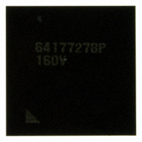
HD6417727BP160CV
Manufacturer Part Number
HD6417727BP160CV
Description
IC SH MPU ROMLESS 240BGA
Manufacturer
Renesas Electronics America
Series
SuperH® SH7700r
Datasheet
1.HD6417727BP100CV.pdf
(1098 pages)
Specifications of HD6417727BP160CV
Core Processor
SH-3 DSP
Core Size
32-Bit
Speed
160MHz
Connectivity
FIFO, SCI, SIO, SmartCard, USB
Peripherals
DMA, LCD, POR, WDT
Number Of I /o
104
Program Memory Type
ROMless
Ram Size
32K x 8
Voltage - Supply (vcc/vdd)
1.7 V ~ 2.05 V
Data Converters
A/D 6x10b; D/A 2x8b
Oscillator Type
Internal
Operating Temperature
-20°C ~ 75°C
Package / Case
240-BGA
Package
240CSP
Family Name
SuperH
Maximum Speed
160 MHz
Operating Supply Voltage
1.8|3.3 V
Data Bus Width
32 Bit
Number Of Programmable I/os
104
Interface Type
SCI/USB
On-chip Adc
6-chx10-bit
On-chip Dac
2-chx8-bit
Number Of Timers
4
Lead Free Status / RoHS Status
Lead free / RoHS Compliant
Eeprom Size
-
Program Memory Size
-
Available stocks
Company
Part Number
Manufacturer
Quantity
Price
Company:

Part Number:
HD6417727BP160CV
Manufacturer:
LITEON
Quantity:
46 000
Company:
Part Number:
HD6417727BP160CV
Manufacturer:
Renesas Electronics America
Quantity:
10 000


21.2.9
TDFP is the write only port for transmit FIFO. Transmit FIFO has 128 stages (maximum), and can
generate interrupt of the data empty as well as of the threshold size specified by FFSZ (ACTR1).
Directly after the reset and when TE (ACTR1) bit is 0, the pointer of FIFO is set to the first
address and data becomes empty. The interrupt will occur when the TE bit (ACTR1) is written to
1 at that state. In normal case, TE bit should be changed after writing data into transmit FIFO.
21.2.10 Receive Data FIFO Port (RDFP)
RDFP is the read only register for receive FIFO. Receive FIFO has 128 stages (maximum), and
can generate interrupt of the data full as well as of the threshold size specified by FFSZ (ACTR1).
Directly after the reset and when RE bit (ACTR1) is 0, the pointer of FIFO is fixed at the first
address and data from RDFP becomes undetermined.
21.3
21.3.1
AFE interface module generates 3 types of interrupt: FIFO data transfer, ringing detect, and dial
pulse transmit end. The timing of each interruption is described below.
(1) FIFO Interrupt Timing
Figure 21.2 shows interrupt timing of data transfer FIFO. Transmit FIFO generates the TFE and
THE interrupts after the last data is transfer red shift register. Receive FIFO generates the RFF and
RHF interrupt after the last data or specified word is transferred from shift register to FIFO.
Initial value:
Initial value:
R/W:
R/W:
Transmit Data FIFO Port (TDFP)
Operation
Interrupt Timing
Bit:
Bit:
15
15
W
R
∗
∗
14
14
W
R
∗
∗
13
13
W
R
∗
∗
12
12
W
R
∗
∗
11
11
W
R
∗
∗
10
10
W
R
∗
∗
W
R
9
9
∗
∗
Section 21 Analog Front End Interface (AFEIF)
W
R
8
8
∗
∗
RDFP
TDFP
Rev.6.00 Mar. 27, 2009 Page 671 of 1036
W
R
7
7
∗
∗
W
R
6
6
∗
∗
W
R
5
∗
5
∗
W
R
4
∗
4
∗
W
R
3
3
∗
∗
REJ09B0254-0600
W
R
2
2
∗
∗
W
R
1
1
∗
∗
W
R
0
0
∗
∗
Related parts for HD6417727BP160CV
Image
Part Number
Description
Manufacturer
Datasheet
Request
R

Part Number:
Description:
KIT STARTER FOR M16C/29
Manufacturer:
Renesas Electronics America
Datasheet:

Part Number:
Description:
KIT STARTER FOR R8C/2D
Manufacturer:
Renesas Electronics America
Datasheet:

Part Number:
Description:
R0K33062P STARTER KIT
Manufacturer:
Renesas Electronics America
Datasheet:

Part Number:
Description:
KIT STARTER FOR R8C/23 E8A
Manufacturer:
Renesas Electronics America
Datasheet:

Part Number:
Description:
KIT STARTER FOR R8C/25
Manufacturer:
Renesas Electronics America
Datasheet:

Part Number:
Description:
KIT STARTER H8S2456 SHARPE DSPLY
Manufacturer:
Renesas Electronics America
Datasheet:

Part Number:
Description:
KIT STARTER FOR R8C38C
Manufacturer:
Renesas Electronics America
Datasheet:

Part Number:
Description:
KIT STARTER FOR R8C35C
Manufacturer:
Renesas Electronics America
Datasheet:

Part Number:
Description:
KIT STARTER FOR R8CL3AC+LCD APPS
Manufacturer:
Renesas Electronics America
Datasheet:
Part Number:
Description:
KIT STARTER FOR RX610
Manufacturer:
Renesas Electronics America
Datasheet:

Part Number:
Description:
KIT STARTER FOR R32C/118
Manufacturer:
Renesas Electronics America
Datasheet:

Part Number:
Description:
KIT DEV RSK-R8C/26-29
Manufacturer:
Renesas Electronics America
Datasheet:

Part Number:
Description:
KIT STARTER FOR SH7124
Manufacturer:
Renesas Electronics America
Datasheet:

Part Number:
Description:
KIT STARTER FOR H8SX/1622
Manufacturer:
Renesas Electronics America
Datasheet:

Part Number:
Description:
KIT DEV FOR SH7203
Manufacturer:
Renesas Electronics America
Datasheet: