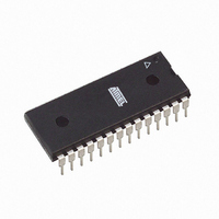
ATMEGA88-20PU Atmel, ATMEGA88-20PU Datasheet - Page 208

ATMEGA88-20PU
Manufacturer Part Number
ATMEGA88-20PU
Description
IC AVR MCU 8K 20MHZ 5V 28DIP
Manufacturer
Atmel
Series
AVR® ATmegar
Specifications of ATMEGA88-20PU
Core Processor
AVR
Core Size
8-Bit
Speed
20MHz
Connectivity
I²C, SPI, UART/USART
Peripherals
Brown-out Detect/Reset, POR, PWM, WDT
Number Of I /o
23
Program Memory Size
8KB (4K x 16)
Program Memory Type
FLASH
Eeprom Size
512 x 8
Ram Size
1K x 8
Voltage - Supply (vcc/vdd)
2.7 V ~ 5.5 V
Data Converters
A/D 6x10b
Oscillator Type
Internal
Operating Temperature
-40°C ~ 85°C
Package / Case
28-DIP (0.300", 7.62mm)
Cpu Family
ATmega
Device Core
AVR
Device Core Size
8b
Frequency (max)
20MHz
Interface Type
SPI/TWI/USART
Total Internal Ram Size
1KB
# I/os (max)
23
Number Of Timers - General Purpose
3
Operating Supply Voltage (typ)
3.3/5V
Operating Supply Voltage (max)
5.5V
Operating Supply Voltage (min)
2.7V
On-chip Adc
6-chx10-bit
Instruction Set Architecture
RISC
Operating Temp Range
-40C to 85C
Operating Temperature Classification
Industrial
Mounting
Through Hole
Pin Count
28
Package Type
PDIP
Processor Series
ATMEGA8x
Core
AVR8
Data Bus Width
8 bit
Data Ram Size
1 KB
Maximum Clock Frequency
20 MHz
Number Of Programmable I/os
23
Number Of Timers
3
Operating Supply Voltage
2.7 V to 5.5 V
Maximum Operating Temperature
+ 85 C
Mounting Style
Through Hole
3rd Party Development Tools
EWAVR, EWAVR-BL
Development Tools By Supplier
ATAVRDRAGON, ATSTK500, ATSTK600, ATAVRISP2, ATAVRONEKIT, ATAVRTS2080A, ATASTK512-EK1-IND
Minimum Operating Temperature
- 40 C
Package
28PDIP
Family Name
ATmega
Maximum Speed
20 MHz
For Use With
ATAVRDRAGON - KIT DRAGON 32KB FLASH MEM AVRATAVRISP2 - PROGRAMMER AVR IN SYSTEM
Lead Free Status / RoHS Status
Lead free / RoHS Compliant
- Current page: 208 of 378
- Download datasheet (8Mb)
21. 2-wire Serial Interface
21.1
21.2
21.2.1
208
Features
2-wire Serial Interface Bus Definition
ATmega48/88/168
TWI Terminology
•
•
•
•
•
•
•
•
•
•
•
The 2-wire Serial Interface (TWI) is ideally suited for typical microcontroller applications. The
TWI protocol allows the systems designer to interconnect up to 128 different devices using only
two bi-directional bus lines, one for clock (SCL) and one for data (SDA). The only external hard-
ware needed to implement the bus is a single pull-up resistor for each of the TWI bus lines. All
devices connected to the bus have individual addresses, and mechanisms for resolving bus
contention are inherent in the TWI protocol.
Figure 21-1. TWI Bus Interconnection
The following definitions are frequently encountered in this section.
Table 21-1.
Term
Master
Simple Yet Powerful and Flexible Communication Interface, only two Bus Lines Needed
Both Master and Slave Operation Supported
Device can Operate as Transmitter or Receiver
7-bit Address Space Allows up to 128 Different Slave Addresses
Multi-master Arbitration Support
Up to 400 kHz Data Transfer Speed
Slew-rate Limited Output Drivers
Noise Suppression Circuitry Rejects Spikes on Bus Lines
Fully Programmable Slave Address with General Call Support
Address Recognition Causes Wake-up When AVR is in Sleep Mode
Compatible with Philips I
SDA
SCL
TWI Terminology
Description
The device that initiates and terminates a transmission. The Master also generates the
SCL clock.
Device 1
2
C protocol
Device 2
Device 3
........
Device n
V
CC
R1
R2
2545S–AVR–07/10
Related parts for ATMEGA88-20PU
Image
Part Number
Description
Manufacturer
Datasheet
Request
R

Part Number:
Description:
IC MCU AVR 8K 5V 20MHZ 32-TQFP
Manufacturer:
Atmel
Datasheet:

Part Number:
Description:
Manufacturer:
Atmel Corporation
Datasheet:

Part Number:
Description:
Manufacturer:
Atmel Corporation
Datasheet:

Part Number:
Description:
MCU AVR 8K FLASH 15MHZ 32-QFN
Manufacturer:
Atmel
Datasheet:

Part Number:
Description:
IC AVR MCU 8K 20MHZ 5V 32TQFP
Manufacturer:
Atmel
Datasheet:

Part Number:
Description:
IC AVR MCU 8K 20MHZ 5V 32-QFN
Manufacturer:
Atmel
Datasheet:

Part Number:
Description:
IC MCU AVR 8K 5V 20MHZ 32-TQFP
Manufacturer:
Atmel
Datasheet:

Part Number:
Description:
IC MCU AVR 8K 5V 20MHZ 32-QFN
Manufacturer:
Atmel
Datasheet:

Part Number:
Description:
IC MCU AVR 8K 5V 20MHZ 32-QFN
Manufacturer:
Atmel
Datasheet:

Part Number:
Description:
IC MCU AVR 8K 5V 20MHZ 28-DIP
Manufacturer:
Atmel
Datasheet:

Part Number:
Description:
IC MCU AVR 8K 5V 20MHZ 28-DIP
Manufacturer:
Atmel
Datasheet:

Part Number:
Description:
MCU AVR 8K FLASH 20MHZ 32TQFP
Manufacturer:
Atmel
Datasheet:

Part Number:
Description:
MCU AVR 8K FLASH 20MHZ 32QFN
Manufacturer:
Atmel
Datasheet:


