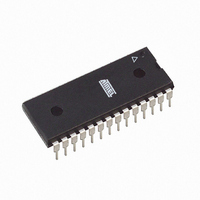
ATMEGA88-20PU Atmel, ATMEGA88-20PU Datasheet - Page 86

ATMEGA88-20PU
Manufacturer Part Number
ATMEGA88-20PU
Description
IC AVR MCU 8K 20MHZ 5V 28DIP
Manufacturer
Atmel
Series
AVR® ATmegar
Specifications of ATMEGA88-20PU
Core Processor
AVR
Core Size
8-Bit
Speed
20MHz
Connectivity
I²C, SPI, UART/USART
Peripherals
Brown-out Detect/Reset, POR, PWM, WDT
Number Of I /o
23
Program Memory Size
8KB (4K x 16)
Program Memory Type
FLASH
Eeprom Size
512 x 8
Ram Size
1K x 8
Voltage - Supply (vcc/vdd)
2.7 V ~ 5.5 V
Data Converters
A/D 6x10b
Oscillator Type
Internal
Operating Temperature
-40°C ~ 85°C
Package / Case
28-DIP (0.300", 7.62mm)
Cpu Family
ATmega
Device Core
AVR
Device Core Size
8b
Frequency (max)
20MHz
Interface Type
SPI/TWI/USART
Total Internal Ram Size
1KB
# I/os (max)
23
Number Of Timers - General Purpose
3
Operating Supply Voltage (typ)
3.3/5V
Operating Supply Voltage (max)
5.5V
Operating Supply Voltage (min)
2.7V
On-chip Adc
6-chx10-bit
Instruction Set Architecture
RISC
Operating Temp Range
-40C to 85C
Operating Temperature Classification
Industrial
Mounting
Through Hole
Pin Count
28
Package Type
PDIP
Processor Series
ATMEGA8x
Core
AVR8
Data Bus Width
8 bit
Data Ram Size
1 KB
Maximum Clock Frequency
20 MHz
Number Of Programmable I/os
23
Number Of Timers
3
Operating Supply Voltage
2.7 V to 5.5 V
Maximum Operating Temperature
+ 85 C
Mounting Style
Through Hole
3rd Party Development Tools
EWAVR, EWAVR-BL
Development Tools By Supplier
ATAVRDRAGON, ATSTK500, ATSTK600, ATAVRISP2, ATAVRONEKIT, ATAVRTS2080A, ATASTK512-EK1-IND
Minimum Operating Temperature
- 40 C
Package
28PDIP
Family Name
ATmega
Maximum Speed
20 MHz
For Use With
ATAVRDRAGON - KIT DRAGON 32KB FLASH MEM AVRATAVRISP2 - PROGRAMMER AVR IN SYSTEM
Lead Free Status / RoHS Status
Lead free / RoHS Compliant
- Current page: 86 of 378
- Download datasheet (8Mb)
13.4
13.4.1
13.4.2
13.4.3
13.4.4
13.4.5
13.4.6
13.4.7
86
Register Description
ATmega48/88/168
MCUCR – MCU Control Register
PORTB – The Port B Data Register
DDRB – The Port B Data Direction Register
PINB – The Port B Input Pins Address
PORTC – The Port C Data Register
DDRC – The Port C Data Direction Register
PINC – The Port C Input Pins Address
• Bit 4 – PUD: Pull-up Disable
When this bit is written to one, the pull-ups in the I/O ports are disabled even if the DDxn and
PORTxn Registers are configured to enable the pull-ups ({DDxn, PORTxn} = 0b01). See
figuring the Pin” on page 71
Bit
0x35 (0x55)
Read/Write
Initial Value
Bit
0x05 (0x25)
Read/Write
Initial Value
Bit
0x04 (0x24)
Read/Write
Initial Value
Bit
0x03 (0x23)
Read/Write
Initial Value
Bit
0x08 (0x28)
Read/Write
Initial Value
Bit
0x07 (0x27)
Read/Write
Initial Value
Bit
0x06 (0x26)
Read/Write
Initial Value
PORTB7
PINB7
DDB7
R/W
R/W
N/A
R
7
–
0
R
R
R
R
7
0
7
0
7
7
–
0
7
–
0
7
–
0
PORTB6
PORTC6
PINB6
PINC6
DDB6
DDC6
R/W
R/W
R/W
R/W
N/A
N/A
R
R
R
6
–
0
6
0
6
0
6
6
0
6
0
6
for more details about this feature.
PORTB5
PORTC5
PINB5
PINC5
DDB5
DDC5
R/W
R/W
R/W
R/W
N/A
N/A
R
R
5
0
5
0
5
5
0
5
0
5
R
5
–
0
PORTB4
PORTC4
PINB4
PINC4
DDB4
DDC4
R/W
R/W
R/W
R/W
N/A
N/A
R
R
4
0
4
0
4
4
0
4
0
4
PUD
R/W
4
0
PORTB3
PORTC3
PINB3
PINC3
DDB3
DDC3
R/W
R/W
R/W
R/W
N/A
N/A
R
R
3
0
3
0
3
3
0
3
0
3
R
3
–
0
PORTB2
PORTC2
PINB2
PINC2
DDB2
DDC2
R/W
R/W
R/W
R/W
N/A
N/A
R
R
2
0
2
0
2
2
0
2
0
2
R
2
–
0
PORTB1
PORTC1
PINB1
PINC1
DDB1
DDC1
R/W
R/W
R/W
R/W
IVSEL
N/A
N/A
R/W
R
R
1
0
1
0
1
1
0
1
0
1
1
0
PORTB0
PORTC0
PINB0
PINC0
DDB0
DDC0
IVCE
R/W
R/W
R/W
R/W
R/W
N/A
N/A
R
R
0
0
0
0
0
0
0
0
0
0
0
0
2545S–AVR–07/10
MCUCR
PORTB
PORTC
DDRB
DDRC
PINB
PINC
“Con-
Related parts for ATMEGA88-20PU
Image
Part Number
Description
Manufacturer
Datasheet
Request
R

Part Number:
Description:
IC MCU AVR 8K 5V 20MHZ 32-TQFP
Manufacturer:
Atmel
Datasheet:

Part Number:
Description:
Manufacturer:
Atmel Corporation
Datasheet:

Part Number:
Description:
Manufacturer:
Atmel Corporation
Datasheet:

Part Number:
Description:
MCU AVR 8K FLASH 15MHZ 32-QFN
Manufacturer:
Atmel
Datasheet:

Part Number:
Description:
IC AVR MCU 8K 20MHZ 5V 32TQFP
Manufacturer:
Atmel
Datasheet:

Part Number:
Description:
IC AVR MCU 8K 20MHZ 5V 32-QFN
Manufacturer:
Atmel
Datasheet:

Part Number:
Description:
IC MCU AVR 8K 5V 20MHZ 32-TQFP
Manufacturer:
Atmel
Datasheet:

Part Number:
Description:
IC MCU AVR 8K 5V 20MHZ 32-QFN
Manufacturer:
Atmel
Datasheet:

Part Number:
Description:
IC MCU AVR 8K 5V 20MHZ 32-QFN
Manufacturer:
Atmel
Datasheet:

Part Number:
Description:
IC MCU AVR 8K 5V 20MHZ 28-DIP
Manufacturer:
Atmel
Datasheet:

Part Number:
Description:
IC MCU AVR 8K 5V 20MHZ 28-DIP
Manufacturer:
Atmel
Datasheet:

Part Number:
Description:
MCU AVR 8K FLASH 20MHZ 32TQFP
Manufacturer:
Atmel
Datasheet:

Part Number:
Description:
MCU AVR 8K FLASH 20MHZ 32QFN
Manufacturer:
Atmel
Datasheet:


