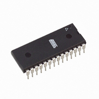
ATMEGA88-20PU Atmel, ATMEGA88-20PU Datasheet - Page 83

ATMEGA88-20PU
Manufacturer Part Number
ATMEGA88-20PU
Description
IC AVR MCU 8K 20MHZ 5V 28DIP
Manufacturer
Atmel
Series
AVR® ATmegar
Specifications of ATMEGA88-20PU
Core Processor
AVR
Core Size
8-Bit
Speed
20MHz
Connectivity
I²C, SPI, UART/USART
Peripherals
Brown-out Detect/Reset, POR, PWM, WDT
Number Of I /o
23
Program Memory Size
8KB (4K x 16)
Program Memory Type
FLASH
Eeprom Size
512 x 8
Ram Size
1K x 8
Voltage - Supply (vcc/vdd)
2.7 V ~ 5.5 V
Data Converters
A/D 6x10b
Oscillator Type
Internal
Operating Temperature
-40°C ~ 85°C
Package / Case
28-DIP (0.300", 7.62mm)
Cpu Family
ATmega
Device Core
AVR
Device Core Size
8b
Frequency (max)
20MHz
Interface Type
SPI/TWI/USART
Total Internal Ram Size
1KB
# I/os (max)
23
Number Of Timers - General Purpose
3
Operating Supply Voltage (typ)
3.3/5V
Operating Supply Voltage (max)
5.5V
Operating Supply Voltage (min)
2.7V
On-chip Adc
6-chx10-bit
Instruction Set Architecture
RISC
Operating Temp Range
-40C to 85C
Operating Temperature Classification
Industrial
Mounting
Through Hole
Pin Count
28
Package Type
PDIP
Processor Series
ATMEGA8x
Core
AVR8
Data Bus Width
8 bit
Data Ram Size
1 KB
Maximum Clock Frequency
20 MHz
Number Of Programmable I/os
23
Number Of Timers
3
Operating Supply Voltage
2.7 V to 5.5 V
Maximum Operating Temperature
+ 85 C
Mounting Style
Through Hole
3rd Party Development Tools
EWAVR, EWAVR-BL
Development Tools By Supplier
ATAVRDRAGON, ATSTK500, ATSTK600, ATAVRISP2, ATAVRONEKIT, ATAVRTS2080A, ATASTK512-EK1-IND
Minimum Operating Temperature
- 40 C
Package
28PDIP
Family Name
ATmega
Maximum Speed
20 MHz
For Use With
ATAVRDRAGON - KIT DRAGON 32KB FLASH MEM AVRATAVRISP2 - PROGRAMMER AVR IN SYSTEM
Lead Free Status / RoHS Status
Lead free / RoHS Compliant
- Current page: 83 of 378
- Download datasheet (8Mb)
13.3.3
2545S–AVR–07/10
Alternate Functions of Port D
The Port D pins with alternate functions are shown in
Table 13-9.
The alternate pin configuration is as follows:
• AIN1/OC2B/PCINT23 – Port D, Bit 7
AIN1, Analog Comparator Negative Input. Configure the port pin as input with the internal pull-up
switched off to avoid the digital port function from interfering with the function of the Analog
Comparator.
PCINT23: Pin Change Interrupt source 23. The PD7 pin can serve as an external interrupt
source.
• AIN0/OC0A/PCINT22 – Port D, Bit 6
AIN0, Analog Comparator Positive Input. Configure the port pin as input with the internal pull-up
switched off to avoid the digital port function from interfering with the function of the Analog
Comparator.
OC0A, Output Compare Match output: The PD6 pin can serve as an external output for the
Timer/Counter0 Compare Match A. The PD6 pin has to be configured as an output (DDD6 set
(one)) to serve this function. The OC0A pin is also the output pin for the PWM mode timer
function.
PCINT22: Pin Change Interrupt source 22. The PD6 pin can serve as an external interrupt
source.
Port Pin
PD7
PD6
PD5
PD4
PD3
PD2
PD1
PD0
Port D Pins Alternate Functions
Alternate Function
AIN1 (Analog Comparator Negative Input)
PCINT23 (Pin Change Interrupt 23)
AIN0 (Analog Comparator Positive Input)
OC0A (Timer/Counter0 Output Compare Match A Output)
PCINT22 (Pin Change Interrupt 22)
T1 (Timer/Counter 1 External Counter Input)
OC0B (Timer/Counter0 Output Compare Match B Output)
PCINT21 (Pin Change Interrupt 21)
XCK (USART External Clock Input/Output)
T0 (Timer/Counter 0 External Counter Input)
PCINT20 (Pin Change Interrupt 20)
INT1 (External Interrupt 1 Input)
OC2B (Timer/Counter2 Output Compare Match B Output)
PCINT19 (Pin Change Interrupt 19)
INT0 (External Interrupt 0 Input)
PCINT18 (Pin Change Interrupt 18)
TXD (USART Output Pin)
PCINT17 (Pin Change Interrupt 17)
RXD (USART Input Pin)
PCINT16 (Pin Change Interrupt 16)
Table
13-9.
ATmega48/88/168
83
Related parts for ATMEGA88-20PU
Image
Part Number
Description
Manufacturer
Datasheet
Request
R

Part Number:
Description:
IC MCU AVR 8K 5V 20MHZ 32-TQFP
Manufacturer:
Atmel
Datasheet:

Part Number:
Description:
Manufacturer:
Atmel Corporation
Datasheet:

Part Number:
Description:
Manufacturer:
Atmel Corporation
Datasheet:

Part Number:
Description:
MCU AVR 8K FLASH 15MHZ 32-QFN
Manufacturer:
Atmel
Datasheet:

Part Number:
Description:
IC AVR MCU 8K 20MHZ 5V 32TQFP
Manufacturer:
Atmel
Datasheet:

Part Number:
Description:
IC AVR MCU 8K 20MHZ 5V 32-QFN
Manufacturer:
Atmel
Datasheet:

Part Number:
Description:
IC MCU AVR 8K 5V 20MHZ 32-TQFP
Manufacturer:
Atmel
Datasheet:

Part Number:
Description:
IC MCU AVR 8K 5V 20MHZ 32-QFN
Manufacturer:
Atmel
Datasheet:

Part Number:
Description:
IC MCU AVR 8K 5V 20MHZ 32-QFN
Manufacturer:
Atmel
Datasheet:

Part Number:
Description:
IC MCU AVR 8K 5V 20MHZ 28-DIP
Manufacturer:
Atmel
Datasheet:

Part Number:
Description:
IC MCU AVR 8K 5V 20MHZ 28-DIP
Manufacturer:
Atmel
Datasheet:

Part Number:
Description:
MCU AVR 8K FLASH 20MHZ 32TQFP
Manufacturer:
Atmel
Datasheet:

Part Number:
Description:
MCU AVR 8K FLASH 20MHZ 32QFN
Manufacturer:
Atmel
Datasheet:


