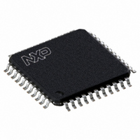
P89CV51RC2FBC,557 NXP Semiconductors, P89CV51RC2FBC,557 Datasheet - Page 40

P89CV51RC2FBC,557
Manufacturer Part Number
P89CV51RC2FBC,557
Description
IC 80C51 MCU FLASH 64K 44-TQFP
Manufacturer
NXP Semiconductors
Series
89Cr
Datasheet
1.P89CV51RB2FA512.pdf
(76 pages)
Specifications of P89CV51RC2FBC,557
Program Memory Type
FLASH
Program Memory Size
32KB (32K x 8)
Package / Case
44-TQFP, 44-VQFP
Core Processor
8051
Core Size
8-Bit
Speed
40MHz
Connectivity
EBI/EMI, SPI, UART/USART
Peripherals
POR, PWM, WDT
Number Of I /o
32
Ram Size
1K x 8
Voltage - Supply (vcc/vdd)
4.5 V ~ 5.5 V
Oscillator Type
Internal
Operating Temperature
-40°C ~ 85°C
Processor Series
P89CV5x
Core
80C51
Data Bus Width
8 bit
Data Ram Size
1 KB
Interface Type
SPI/UART
Maximum Clock Frequency
40 MHz
Number Of Programmable I/os
32
Number Of Timers
3
Operating Supply Voltage
4.5 V to 5.5 V
Maximum Operating Temperature
+ 85 C
Mounting Style
SMD/SMT
3rd Party Development Tools
PK51, CA51, A51, ULINK2
Minimum Operating Temperature
- 40 C
Lead Free Status / RoHS Status
Lead free / RoHS Compliant
Eeprom Size
-
Data Converters
-
Lead Free Status / Rohs Status
Lead free / RoHS Compliant
Other names
568-4255
935284104557
P89CV51RC2FBC
935284104557
P89CV51RC2FBC
Available stocks
Company
Part Number
Manufacturer
Quantity
Price
Company:
Part Number:
P89CV51RC2FBC,557
Manufacturer:
NXP Semiconductors
Quantity:
10 000
NXP Semiconductors
P89CV51RB2_RC2_RD2_3
Product data sheet
The following examples help to show the versatility of this scheme.
Example 1, slave 0:
Example 2, slave 1:
In the above example SADDR is the same and the SADEN data is used to differentiate
between the two slaves. Slave 0 requires a 0 in bit 0 and it ignores bit 1. Slave 1 requires
a 0 in bit 1 and bit 0 is ignored. A unique address for slave 0 would be 1100 0010 since
slave 1 requires a 0 in bit 1. A unique address for slave 1 would be 1100 0001 since a 1 in
bit 0 will exclude slave 0. Both slaves can be selected at the same time by an address
which has bit 0 = 0 (for slave 0) and bit 1 = 0 (for slave 1). Thus, both could be addressed
with 1100 0000.
In a more complex system the following could be used to select slaves 1 and 2 while
excluding slave 0.
Example 1, slave 0:
SADDR = 1100 0000
--------------------------------------------------- -
Example 2, slave 1:
SADDR = 1110 0000
--------------------------------------------------- -
Example 3, slave 2:
SADDR = 1100 0000
--------------------------------------------------- -
In the above example the differentiation among the 3 slaves is in the lower 3 address bits.
Slave 0 requires that bit 0 = 0 and it can be uniquely addressed by 1110 0110. Slave 1
requires that bit 1 = 0 and it can be uniquely addressed by 1110 0101. Slave 2 requires
that bit 2 = 0 and its unique address is 1110 0011. To select slaves 0 and 1 and exclude
slave 2 use address 1110 0100, since it is necessary to make bit 2 = 1 to exclude slave 2.
The broadcast address for each slave is created by taking the logical OR of SADDR and
SADEN. Zeros in this result are treated as don’t cares. In most cases, interpreting the
don’t-cares as ones, the broadcast address will be FFH. Upon reset SADDR and SADEN
are loaded with 0s. This produces a given address of all don’t cares as well as a broadcast
SADEN = 1111 1001
SADEN = 1111 1010
SADEN = 1111 1100
SADDR = 1100 0000
--------------------------------------------------- -
SADDR = 1100 0000
--------------------------------------------------- -
SADEN = 1111 1101
SADEN = 1111 1110
Given = 1100 0XX0
Given = 1110 0X0X
Given = 1100 00XX
Given = 1100 00X0
Given = 1100 000X
Rev. 03 — 25 August 2009
P89CV51RB2/RC2/RD2
80C51 with 1 kB RAM, SPI
© NXP B.V. 2009. All rights reserved.
40 of 76


