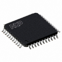
P89CV51RC2FBC,557 NXP Semiconductors, P89CV51RC2FBC,557 Datasheet - Page 42

P89CV51RC2FBC,557
Manufacturer Part Number
P89CV51RC2FBC,557
Description
IC 80C51 MCU FLASH 64K 44-TQFP
Manufacturer
NXP Semiconductors
Series
89Cr
Datasheet
1.P89CV51RB2FA512.pdf
(76 pages)
Specifications of P89CV51RC2FBC,557
Program Memory Type
FLASH
Program Memory Size
32KB (32K x 8)
Package / Case
44-TQFP, 44-VQFP
Core Processor
8051
Core Size
8-Bit
Speed
40MHz
Connectivity
EBI/EMI, SPI, UART/USART
Peripherals
POR, PWM, WDT
Number Of I /o
32
Ram Size
1K x 8
Voltage - Supply (vcc/vdd)
4.5 V ~ 5.5 V
Oscillator Type
Internal
Operating Temperature
-40°C ~ 85°C
Processor Series
P89CV5x
Core
80C51
Data Bus Width
8 bit
Data Ram Size
1 KB
Interface Type
SPI/UART
Maximum Clock Frequency
40 MHz
Number Of Programmable I/os
32
Number Of Timers
3
Operating Supply Voltage
4.5 V to 5.5 V
Maximum Operating Temperature
+ 85 C
Mounting Style
SMD/SMT
3rd Party Development Tools
PK51, CA51, A51, ULINK2
Minimum Operating Temperature
- 40 C
Lead Free Status / RoHS Status
Lead free / RoHS Compliant
Eeprom Size
-
Data Converters
-
Lead Free Status / Rohs Status
Lead free / RoHS Compliant
Other names
568-4255
935284104557
P89CV51RC2FBC
935284104557
P89CV51RC2FBC
Available stocks
Company
Part Number
Manufacturer
Quantity
Price
Company:
Part Number:
P89CV51RC2FBC,557
Manufacturer:
NXP Semiconductors
Quantity:
10 000
NXP Semiconductors
P89CV51RB2_RC2_RD2_3
Product data sheet
Fig 16. SPI master-slave interconnection
CLOCK GENERATOR
SPI
Table 27.
Reset source(s): any reset; reset value: 0000 0000B.
Table 28.
Table 29.
Bit
Symbol
Bit
7
6
5
4
3
2
1
0
SPR1
0
0
1
1
8-BIT SHIFT REGISTER
MSB master LSB
Symbol
SPIE
SPEN
DORD
MSTR
CPOL
CPHA
SPR1
SPR0
SPCR - SPI control register (address D5H) bit allocation
SPCR - SPI control register (address D5H) bit description
SPCR - SPI control register (address D5H) clock rate selection
SPIE
7
Description
SPI interrupt enable. If both SPIE = 1 and ES = 1, SPI interrupts are enabled.
SPI enable bit. When set enables SPI.
Data transmission order. 0 = MSB first; 1 = LSB first in data transmission.
Master/Slave select. 1 = Master mode, 0 = Slave mode.
Clock polarity. 1 = SPICLK is HIGH when idle (active LOW), 0 = SPICLK is
LOW when idle (active HIGH).
Clock Phase control bit. 1 = shift-triggered on the trailing edge of the clock;
0 = shift-triggered on the leading edge of the clock.
SPI clock Rate select bit 1. Along with SPR0 controls the SPICLK rate of the
device when a master. SPR1 and SPR0 have no effect on the slave; see
Table
SPI clock Rate select bit 0. Along with SPR1 controls the SPICLK rate of the
device when a master. SPR1 and SPR0 have no effect on the slave; see
Table
SPR0
0
1
0
1
Rev. 03 — 25 August 2009
SPEN
29.
29.
6
DORD
SCK
MISO
MOSI
SS
V
5
DD
SPICLK = f
6-clock mode
2
8
32
64
V
MISO
MOSI
P89CV51RB2/RC2/RD2
SS
SCK
SS
MSTR
4
osc
divided by
CPOL
3
8-BIT SHIFT REGISTER
MSB slave LSB
80C51 with 1 kB RAM, SPI
CPHA
12-clock mode
4
16
64
128
2
© NXP B.V. 2009. All rights reserved.
SPR1
002aaa528
1
SPR0
42 of 76
0


