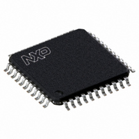
P89CV51RC2FBC,557 NXP Semiconductors, P89CV51RC2FBC,557 Datasheet - Page 5

P89CV51RC2FBC,557
Manufacturer Part Number
P89CV51RC2FBC,557
Description
IC 80C51 MCU FLASH 64K 44-TQFP
Manufacturer
NXP Semiconductors
Series
89Cr
Datasheet
1.P89CV51RB2FA512.pdf
(76 pages)
Specifications of P89CV51RC2FBC,557
Program Memory Type
FLASH
Program Memory Size
32KB (32K x 8)
Package / Case
44-TQFP, 44-VQFP
Core Processor
8051
Core Size
8-Bit
Speed
40MHz
Connectivity
EBI/EMI, SPI, UART/USART
Peripherals
POR, PWM, WDT
Number Of I /o
32
Ram Size
1K x 8
Voltage - Supply (vcc/vdd)
4.5 V ~ 5.5 V
Oscillator Type
Internal
Operating Temperature
-40°C ~ 85°C
Processor Series
P89CV5x
Core
80C51
Data Bus Width
8 bit
Data Ram Size
1 KB
Interface Type
SPI/UART
Maximum Clock Frequency
40 MHz
Number Of Programmable I/os
32
Number Of Timers
3
Operating Supply Voltage
4.5 V to 5.5 V
Maximum Operating Temperature
+ 85 C
Mounting Style
SMD/SMT
3rd Party Development Tools
PK51, CA51, A51, ULINK2
Minimum Operating Temperature
- 40 C
Lead Free Status / RoHS Status
Lead free / RoHS Compliant
Eeprom Size
-
Data Converters
-
Lead Free Status / Rohs Status
Lead free / RoHS Compliant
Other names
568-4255
935284104557
P89CV51RC2FBC
935284104557
P89CV51RC2FBC
Available stocks
Company
Part Number
Manufacturer
Quantity
Price
Company:
Part Number:
P89CV51RC2FBC,557
Manufacturer:
NXP Semiconductors
Quantity:
10 000
NXP Semiconductors
Table 3.
P89CV51RB2_RC2_RD2_3
Product data sheet
Symbol
P0[0] to P0[7]
P0[0]/AD0
P0[1]/AD1
P0[2]/AD2
P0[3]/AD3
P0[4]/AD4
P0[5]/AD5
P89CV51RB2/RC2/RD2 Pin description
Pin
PLCC44
43
42
41
40
39
38
5.2 Pin description
Fig 3.
TQFP44
37
36
35
34
33
32
TQFP44 pin configuration
Type
I/O
I/O
I/O
I/O
I/O
I/O
I/O
I/O
I/O
I/O
I/O
I/O
I/O
P1[7]/CEX4/SPICLK
P1[5]/CEX2/MOSI
P1[6]/CEX3/MISO
P3[2]/INT0
P3[3]/INT1
P3[0]/RXD
P3[1]/TXD
Description
Port 0: Port 0 is an 8-bit open-drain bidirectional I/O port. Port 0 pins that
have 1s written to them float, and in this state can be used as
high-impedance inputs. Port 0 is also the multiplexed low-order address
and data bus during accesses to external code and data memory. In this
application, it uses strong internal pull-ups when transitioning to 1s.
External pull-ups are required when used as a general purpose I/O port.
P0[0] — Port 0 bit 0.
AD0 — Address/data bit 0.
P0[1] — Port 0 bit 1.
AD1 — Address/data bit 1.
P0[2] — Port 0 bit 2.
AD2 — Address/data bit 2.
P0[3] — Port 0 bit 3.
AD3 — Address/data bit 3.
P0[4] — Port 0 bit 4.
AD4 — Address/data bit 4.
P0[5] — Port 0 bit 5.
AD5 — Address/data bit 5.
P3[4]/T0
P3[5]/T1
Rev. 03 — 25 August 2009
RST
n.c.
10
11
1
2
3
4
5
6
7
8
9
P89CV51RB2/RC2/RD2
P89CV51RB2/RC2/RD2
80C51 with 1 kB RAM, SPI
002aac961
33
32
31
30
29
28
27
26
25
24
23
P0[4]/AD4
P0[5]/AD5
P0[6]/AD6
P0[7]/AD7
EA
n.c.
ALE
PSEN
P2[7]/A15
P2[6]/A14
P2[5]/A13
© NXP B.V. 2009. All rights reserved.
5 of 76


