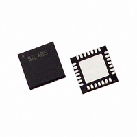
C8051F321 Silicon Laboratories Inc, C8051F321 Datasheet - Page 135

C8051F321
Manufacturer Part Number
C8051F321
Description
IC 8051 MCU 16K FLASH 28MLP
Manufacturer
Silicon Laboratories Inc
Series
C8051F32xr
Datasheet
1.C8051F320R.pdf
(256 pages)
Specifications of C8051F321
Core Processor
8051
Core Size
8-Bit
Speed
25MHz
Connectivity
SMBus (2-Wire/I²C), SPI, UART/USART, USB
Peripherals
Brown-out Detect/Reset, POR, PWM, Temp Sensor, WDT
Number Of I /o
21
Program Memory Size
16KB (16K x 8)
Program Memory Type
FLASH
Ram Size
2.25K x 8
Voltage - Supply (vcc/vdd)
2.7 V ~ 3.6 V
Data Converters
A/D 13x10b
Oscillator Type
Internal
Operating Temperature
-40°C ~ 85°C
Package / Case
28-VQFN Exposed Pad, 28-HVQFN, 28-SQFN, 28-DHVQFN
Lead Free Status / RoHS Status
Contains lead / RoHS non-compliant
Eeprom Size
-
Available stocks
Company
Part Number
Manufacturer
Quantity
Price
Company:
Part Number:
C8051F321
Manufacturer:
SILICON
Quantity:
249
Part Number:
C8051F321
Manufacturer:
SILICON LABS/芯科
Quantity:
20 000
Company:
Part Number:
C8051F321-GM
Manufacturer:
SiliconL
Quantity:
4 364
Part Number:
C8051F321-GM
Manufacturer:
SILICON LABS/芯科
Quantity:
20 000
Part Number:
C8051F321-GMR
Manufacturer:
SILICON LABS/芯科
Quantity:
20 000
- Current page: 135 of 256
- Download datasheet (4Mb)
Bits7-0:
Bits7-0:
P0.7
R/W
R/W
Bit7
Bit7
P0.[7:0]
Write - Output appears on I/O pins per Crossbar Registers (when XBARE = ‘1’).
0: Logic Low Output.
1: Logic High Output (high impedance if corresponding P0MDOUT.n bit = 0).
Read - Always reads ‘0’ if selected as analog input in register P0MDIN. Directly reads Port pin when
configured as digital input.
0: P0.n pin is logic low.
1: P0.n pin is logic high.
Analog Input Configuration Bits for P0.7-P0.0 (respectively).
Port pins configured as analog inputs have their weak pull-up, digital driver, and digital receiver dis-
abled.
0: Corresponding P0.n pin is configured as an analog input.
1: Corresponding P0.n pin is not configured as an analog input.
P0.6
R/W
R/W
Bit6
Bit6
Figure 14.8. P0MDIN: Port0 Input Mode Register
P0.5
R/W
R/W
Bit5
Bit5
Figure 14.7. P0: Port0 Register
P0.4
R/W
R/W
Bit4
Bit4
P0.3
R/W
R/W
Bit3
Bit3
Rev. 1.1
P0.2
R/W
R/W
Bit2
Bit2
P0.1
R/W
R/W
Bit1
Bit1
C8051F320/1
(bit addressable)
P0.0
R/W
R/W
Bit0
Bit0
SFR Address:
SFR Address:
Reset Value
Reset Value
11111111
11111111
0xF1
0x80
135
Related parts for C8051F321
Image
Part Number
Description
Manufacturer
Datasheet
Request
R
Part Number:
Description:
SMD/C°/SINGLE-ENDED OUTPUT SILICON OSCILLATOR
Manufacturer:
Silicon Laboratories Inc
Part Number:
Description:
Manufacturer:
Silicon Laboratories Inc
Datasheet:
Part Number:
Description:
N/A N/A/SI4010 AES KEYFOB DEMO WITH LCD RX
Manufacturer:
Silicon Laboratories Inc
Datasheet:
Part Number:
Description:
N/A N/A/SI4010 SIMPLIFIED KEY FOB DEMO WITH LED RX
Manufacturer:
Silicon Laboratories Inc
Datasheet:
Part Number:
Description:
N/A/-40 TO 85 OC/EZLINK MODULE; F930/4432 HIGH BAND (REV E/B1)
Manufacturer:
Silicon Laboratories Inc
Part Number:
Description:
EZLink Module; F930/4432 Low Band (rev e/B1)
Manufacturer:
Silicon Laboratories Inc
Part Number:
Description:
I°/4460 10 DBM RADIO TEST CARD 434 MHZ
Manufacturer:
Silicon Laboratories Inc
Part Number:
Description:
I°/4461 14 DBM RADIO TEST CARD 868 MHZ
Manufacturer:
Silicon Laboratories Inc
Part Number:
Description:
I°/4463 20 DBM RFSWITCH RADIO TEST CARD 460 MHZ
Manufacturer:
Silicon Laboratories Inc
Part Number:
Description:
I°/4463 20 DBM RADIO TEST CARD 868 MHZ
Manufacturer:
Silicon Laboratories Inc
Part Number:
Description:
I°/4463 27 DBM RADIO TEST CARD 868 MHZ
Manufacturer:
Silicon Laboratories Inc
Part Number:
Description:
I°/4463 SKYWORKS 30 DBM RADIO TEST CARD 915 MHZ
Manufacturer:
Silicon Laboratories Inc
Part Number:
Description:
N/A N/A/-40 TO 85 OC/4463 RFMD 30 DBM RADIO TEST CARD 915 MHZ
Manufacturer:
Silicon Laboratories Inc
Part Number:
Description:
I°/4463 20 DBM RADIO TEST CARD 169 MHZ
Manufacturer:
Silicon Laboratories Inc


