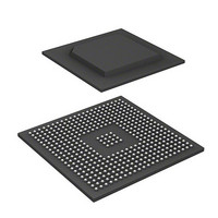
R8A77850ADBGV Renesas Electronics America, R8A77850ADBGV Datasheet - Page 262

R8A77850ADBGV
Manufacturer Part Number
R8A77850ADBGV
Description
IC SUPERH MPU ROMLESS 436-BGA
Manufacturer
Renesas Electronics America
Series
SuperH® SH7780r
Datasheet
1.R8A77850AADBGV.pdf
(1694 pages)
Specifications of R8A77850ADBGV
Core Processor
SH-4A
Core Size
32-Bit
Speed
600MHz
Connectivity
Audio Codec, MMC, Serial Sound, SCI, SIO, SPI, SSI
Peripherals
DMA, POR, WDT
Number Of I /o
108
Program Memory Type
ROMless
Ram Size
8K x 8
Voltage - Supply (vcc/vdd)
1 V ~ 1.2 V
Oscillator Type
External
Operating Temperature
-40°C ~ 85°C
Package / Case
436-BGA
Lead Free Status / RoHS Status
Lead free / RoHS Compliant
Eeprom Size
-
Program Memory Size
-
Data Converters
-
Available stocks
Company
Part Number
Manufacturer
Quantity
Price
Company:
Part Number:
R8A77850ADBGV
Manufacturer:
Renesas Electronics America
Quantity:
10 000
Company:
Part Number:
R8A77850ADBGV#RD0Z
Manufacturer:
Renesas Electronics America
Quantity:
10 000
- Current page: 262 of 1694
- Download datasheet (9Mb)
8. Caches
• FLUSH transaction
(3)
Of the operand cache operating instructions, the coherency control-related specifications of OCBI,
OCBP, and OCBWB have been changed from those of the SH-4A with H'20-valued VER bits in
the processor version register (PVR).
• Changes in the invalidate instruction OCBI@Rn
• Changes in the purge instruction OCBP@Rn
• Changes in the write-back instruction OCBWB@Rn
Rev.1.00 Jan. 10, 2008 Page 230 of 1658
REJ09B0261-0100
When the operand cache is enabled, the FLUSH transaction checks the operand cache and if
the hit line is dirty, then the data is written back to the external memory. If the transaction is
not hit to the cache or the hit entry is not dirty, it is no-operation.
When Rn is designating an address in a non-cacheable area, this instruction is executed as
NOP in the SH-4A with H'20-valued VER bits in the processor version register (PVR). In this
LSI, this instruction invalidates the operand cache line designated by way = Rn[14:13] and
entry = Rn[12:5] provided that Rn[31:24] = H'F4 (OC address array area). In this process,
writing back of the line does not take place even if the line to be invalidated is dirty. This
operation is only executable in privileged mode, and an address error exception occurs in user
mode. TLB-related exceptions do not occur.
Do not execute this instruction to invalidate the memory-mapped array areas and control
register areas for which Rn[31:24] is not H'F4, and their reserved areas (H'F0 to H'F3, H'F5 to
H'FF).
When Rn is designating an address in a non-cacheable area, this instruction is executed as
NOP in the SH-4A with H'20-valued VER bits in the processor version register (PVR). In this
LSI, this instruction invalidates the operand cache line designated by way = Rn[14:13] and
entry = Rn[12:5] provided that Rn[31:24] = H'F4 (OC address array area). In this process,
writing back of the line takes place when the line to be invalidated is dirty. This operation is
only executable in privileged mode, and an address error exception occurs in user mode. TLB-
related exceptions do not occur.
Do not execute this instruction to invalidate the memory-mapped array areas and control
register areas for which Rn[31:24] is not H'F4, and their reserved areas (H'F0 to H'F3, H'F5 to
H'FF).
When Rn is designating an address in a non-cacheable area, this instruction is executed as
NOP in the SH-4A with H'20-valued VER bits in the processor version register (PVR). In this
LSI, provided that Rn[31:24] = H'F4 (OC address array area), this instruction writes back the
operand cache line designated by way = Rn[14:13] and entry = Rn[12:5] if it is dirty and clears
Changes in Instruction Specifications Regarding Coherency Control
Related parts for R8A77850ADBGV
Image
Part Number
Description
Manufacturer
Datasheet
Request
R

Part Number:
Description:
KIT STARTER FOR M16C/29
Manufacturer:
Renesas Electronics America
Datasheet:

Part Number:
Description:
KIT STARTER FOR R8C/2D
Manufacturer:
Renesas Electronics America
Datasheet:

Part Number:
Description:
R0K33062P STARTER KIT
Manufacturer:
Renesas Electronics America
Datasheet:

Part Number:
Description:
KIT STARTER FOR R8C/23 E8A
Manufacturer:
Renesas Electronics America
Datasheet:

Part Number:
Description:
KIT STARTER FOR R8C/25
Manufacturer:
Renesas Electronics America
Datasheet:

Part Number:
Description:
KIT STARTER H8S2456 SHARPE DSPLY
Manufacturer:
Renesas Electronics America
Datasheet:

Part Number:
Description:
KIT STARTER FOR R8C38C
Manufacturer:
Renesas Electronics America
Datasheet:

Part Number:
Description:
KIT STARTER FOR R8C35C
Manufacturer:
Renesas Electronics America
Datasheet:

Part Number:
Description:
KIT STARTER FOR R8CL3AC+LCD APPS
Manufacturer:
Renesas Electronics America
Datasheet:

Part Number:
Description:
KIT STARTER FOR RX610
Manufacturer:
Renesas Electronics America
Datasheet:

Part Number:
Description:
KIT STARTER FOR R32C/118
Manufacturer:
Renesas Electronics America
Datasheet:

Part Number:
Description:
KIT DEV RSK-R8C/26-29
Manufacturer:
Renesas Electronics America
Datasheet:

Part Number:
Description:
KIT STARTER FOR SH7124
Manufacturer:
Renesas Electronics America
Datasheet:

Part Number:
Description:
KIT STARTER FOR H8SX/1622
Manufacturer:
Renesas Electronics America
Datasheet:

Part Number:
Description:
KIT DEV FOR SH7203
Manufacturer:
Renesas Electronics America
Datasheet:


