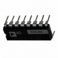
AD625JNZ Analog Devices Inc, AD625JNZ Datasheet - Page 3

AD625JNZ
Manufacturer Part Number
AD625JNZ
Description
IC AMP INST 25MHZ LN 16DIP
Manufacturer
Analog Devices Inc
Type
Low Noiser
Specifications of AD625JNZ
Amplifier Type
Instrumentation
Number Of Circuits
1
Slew Rate
5 V/µs
Gain Bandwidth Product
25MHz
-3db Bandwidth
650kHz
Current - Input Bias
30nA
Voltage - Input Offset
50µV
Current - Supply
3.5mA
Voltage - Supply, Single/dual (±)
±6 V ~ 18 V
Operating Temperature
0°C ~ 70°C
Mounting Type
Through Hole
Package / Case
16-DIP (0.300", 7.62mm)
Bandwidth
650 kHz
Common Mode Rejection Ratio
75
Current, Input Bias
±30 nA
Current, Input Offset
±2 nA
Current, Output
5 mA
Current, Supply
3.5 mA
Number Of Amplifiers
Five
Package Type
PDIP-16
Power Dissipation
450 mW
Resistance, Input
1 Gigaohms
Temperature, Operating, Range
0 to +70 °C
Voltage, Input Offset
50 μV
Voltage, Noise
4 nV/sqrt Hz
Voltage, Output Swing
±10 V
Voltage, Supply
±6 to ±18 V
No. Of Amplifiers
5
Input Offset Voltage
200µV
Gain Db Min
1dB
Amplifier Output
Single Ended
Cmrr
115dB
Supply Voltage Range
± 6V To ± 18V
Rohs Compliant
Yes
Lead Free Status / RoHS Status
Lead free / RoHS Compliant
Output Type
-
Current - Output / Channel
-
Lead Free Status / Rohs Status
RoHS Compliant part
Electrostatic Device
Available stocks
Company
Part Number
Manufacturer
Quantity
Price
Model
NOISE
SENSE INPUT
REFERENCE INPUT
TEMPERATURE RANGE
POWER SUPPLY
NOTES
1
2
Specifications subject to change without notice.
All min and max specifications are guaranteed. Specifications shown in boldface are tested on all production units at final electrical test. Results from those tests are
used to calculate outgoing quality levels.
Gain Error and Gain TC are for the AD625 only. Resistor Network errors will add to the specified errors.
V
Example: G = 10, V
DL
Voltage Noise, 1 kHz
R.T.I., 0.1 Hz to 10 Hz
Current Noise
R
I
Voltage Range
Gain to Output
R
I
Voltage Range
Gain to Output
Specified Performance
Storage
Power Supply Range
Quiescent Current
IN
IN
IN
IN
is the maximum differential input voltage at G = 1 for specified nonlinearity. V
R.T.I.
R.T.O.
G = 1
G = 10
G = 100
G = 1000
0.1 Hz to 10 Hz
J/K Grades
A/B/C Grades
S Grade
D
= 0.50; V
CM
= 12 V – (10/2 × 0.50 V) = 9.5 V.
Min
± 10
± 10
0
–40
–55
–65
AD625A/J/S
Typ
4
75
10
1.0
0.3
0.2
60
10
30
1 ± 0.01
20
30
1 ± 0.01
± 6 to ± 18
3.5
Max
+70
+85
+125
+150
5
Min
± 10
± 10
0
–40
–65
DL
at other gains = 10 V/G. V
AD625B/K
Typ
4
75
10
1.0
0.3
0.2
60
10
30
1 ± 0.01
20
30
1 ± 0.01
± 6 to ± 18
3.5
Max
+70
+85
+150
5
D
= actual differential input voltage.
Min
± 10
± 10
–40
–65
AD625C
Typ
4
75
10
1.0
0.3
0.2
60
10
30
1 ± 0.01
20
30
1 ± 0.01
± 6 to ± 18
3.5
Max
+85
+150
5
AD625
Unit
nV/√Hz
nV/√Hz
µV p-p
µV p-p
µV p-p
µV p-p
pA p-p
kΩ
µA
V
%
kΩ
µA
V
%
°C
°C
°C
°C
V
mA


