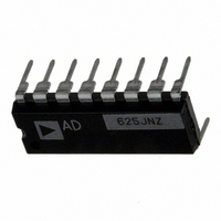
AD625JNZ Analog Devices Inc, AD625JNZ Datasheet - Page 9

AD625JNZ
Manufacturer Part Number
AD625JNZ
Description
IC AMP INST 25MHZ LN 16DIP
Manufacturer
Analog Devices Inc
Type
Low Noiser
Specifications of AD625JNZ
Amplifier Type
Instrumentation
Number Of Circuits
1
Slew Rate
5 V/µs
Gain Bandwidth Product
25MHz
-3db Bandwidth
650kHz
Current - Input Bias
30nA
Voltage - Input Offset
50µV
Current - Supply
3.5mA
Voltage - Supply, Single/dual (±)
±6 V ~ 18 V
Operating Temperature
0°C ~ 70°C
Mounting Type
Through Hole
Package / Case
16-DIP (0.300", 7.62mm)
Bandwidth
650 kHz
Common Mode Rejection Ratio
75
Current, Input Bias
±30 nA
Current, Input Offset
±2 nA
Current, Output
5 mA
Current, Supply
3.5 mA
Number Of Amplifiers
Five
Package Type
PDIP-16
Power Dissipation
450 mW
Resistance, Input
1 Gigaohms
Temperature, Operating, Range
0 to +70 °C
Voltage, Input Offset
50 μV
Voltage, Noise
4 nV/sqrt Hz
Voltage, Output Swing
±10 V
Voltage, Supply
±6 to ±18 V
No. Of Amplifiers
5
Input Offset Voltage
200µV
Gain Db Min
1dB
Amplifier Output
Single Ended
Cmrr
115dB
Supply Voltage Range
± 6V To ± 18V
Rohs Compliant
Yes
Lead Free Status / RoHS Status
Lead free / RoHS Compliant
Output Type
-
Current - Output / Channel
-
Lead Free Status / Rohs Status
RoHS Compliant part
Electrostatic Device
Available stocks
Company
Part Number
Manufacturer
Quantity
Price
Any resistors in series with the inputs of the AD625 will degrade
the noise performance. For this reason the circuit in Figure 26b
should be used if the gains are all greater than 5. For gains less
than 5, either the circuit in Figure 26a or in Figure 26c can be
used. The two 1.4 kΩ resistors in Figure 26a will degrade the
noise performance to:
RESISTOR PROGRAMMABLE GAIN AMPLIFIER
In the resistor-programmed mode (Figure 27), only three exter-
nal resistors are needed to select any gain from 1 to 10,000.
Depending on the application, discrete components or a
pretrimmed network can be used. The gain accuracy and gain
TC are primarily determined by the external resistors since the
AD625C contributes less than 0.02% to gain error and under
5 ppm/°C gain TC. The gain sense current is insensitive to
common-mode voltage, making the CMRR of the resistor pro-
grammed AD625 independent of the match of the two feedback
resistors, R
Selecting Resistor Values
As previously stated each R
stage and sets the unity gain transconductance. These feedback
resistors are provided by the user. The AD625 is tested and
specified with a value of 20 kΩ for R
RTO errors increases with increasing feedback resistance, values
much above 20 kΩ are not recommended (values below 10 kΩ
for R
offset, drift, and bandwidth (Figure 28) when selecting the
feedback resistors. The gain resistor (R
formula R
A list of standard resistors which can be used to set some com-
mon gains is shown in Table I.
For single gain applications, only one offset null adjust is neces-
sary; in these cases the RTI null should be used.
F
may lead to instability). Refer to the graph of RTO noise,
G
F
+GAIN DRIVE
= 2 R
.
SENSE
+GAIN
+V
4 kTR
RTI NULL
RTI NULL
R
S
F
REF
–V
NC
F
S
/(G – l).
ext
G =
1
2
3
4
5
6
7
8
+INPUT
+(4 nV/ Hz )
2R
R
G
F
AD625
10k
+1
10k
F
A1
provides feedback to the input
R
A3
G
A2
10k
10k
2
F
–INPUT
. Since the magnitude of
G
= 7.9 nV / Hz
) is determined by the
16
15
14
13
12
11
10
9
–GAIN DRIVE
+V
RTO
NULL
RTO
NULL
S
–GAIN
SENSE
R
V
F
OUT
SENSE TERMINAL
The sense terminal is the feedback point for the AD625 output
amplifier. Normally it is connected directly to the output. If
heavy load currents are to be drawn through long leads, voltage
drops through lead resistance can cause errors. In these in-
stances the sense terminal can be wired to the load thus putting
Table I. Common Gains Nominally Within
Using Standard 1% Resistors
1000
1024
GAIN
100
200
500
128
256
512
300
200
100
10
20
50
16
32
64
6
5
4
3
2
1
10k
10k
1
2
5
4
8
RTO OFFSET VOLTAGE DRIFT
FEEDBACK RESISTANCE –
FEEDBACK RESISTANCE –
20k
20k
RTO NOISE
30k
30k
40k
40k
50k
50k
R
20 kΩ
19.6 kΩ
20 kΩ
20 kΩ
20 kΩ
19.6 kΩ
20 kΩ
20.5 kΩ
19.6 kΩ
19.6 kΩ
20 kΩ
19.6 kΩ
20 kΩ
19.6 kΩ
20 kΩ
20 kΩ
19.6 kΩ
19.6 kΩ
19.6 kΩ
60k
60k
F
100k
10k
1M
3
2
10k
1
FEEDBACK RESISTANCE –
FEEDBACK RESISTANCE –
RTO OFFSET VOLTAGE
20k
Ω
BANDWIDTH
10
30k
20k
0.5% Error
10k
AD625
40k
50k
100
R
∞
39.2 kΩ
10 kΩ
4.42 kΩ
2.1 kΩ
806 Ω
402 Ω
205 Ω
78.7 Ω
39.2 Ω
13.3 kΩ
5.62 kΩ
2.67 kΩ
1.27 kΩ
634 Ω
316 Ω
154 Ω
76.8 Ω
38.3 Ω
50k
G
60k
1k


