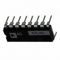
AD625JNZ Analog Devices Inc, AD625JNZ Datasheet - Page 8

AD625JNZ
Manufacturer Part Number
AD625JNZ
Description
IC AMP INST 25MHZ LN 16DIP
Manufacturer
Analog Devices Inc
Type
Low Noiser
Specifications of AD625JNZ
Amplifier Type
Instrumentation
Number Of Circuits
1
Slew Rate
5 V/µs
Gain Bandwidth Product
25MHz
-3db Bandwidth
650kHz
Current - Input Bias
30nA
Voltage - Input Offset
50µV
Current - Supply
3.5mA
Voltage - Supply, Single/dual (±)
±6 V ~ 18 V
Operating Temperature
0°C ~ 70°C
Mounting Type
Through Hole
Package / Case
16-DIP (0.300", 7.62mm)
Bandwidth
650 kHz
Common Mode Rejection Ratio
75
Current, Input Bias
±30 nA
Current, Input Offset
±2 nA
Current, Output
5 mA
Current, Supply
3.5 mA
Number Of Amplifiers
Five
Package Type
PDIP-16
Power Dissipation
450 mW
Resistance, Input
1 Gigaohms
Temperature, Operating, Range
0 to +70 °C
Voltage, Input Offset
50 μV
Voltage, Noise
4 nV/sqrt Hz
Voltage, Output Swing
±10 V
Voltage, Supply
±6 to ±18 V
No. Of Amplifiers
5
Input Offset Voltage
200µV
Gain Db Min
1dB
Amplifier Output
Single Ended
Cmrr
115dB
Supply Voltage Range
± 6V To ± 18V
Rohs Compliant
Yes
Lead Free Status / RoHS Status
Lead free / RoHS Compliant
Output Type
-
Current - Output / Channel
-
Lead Free Status / Rohs Status
RoHS Compliant part
Electrostatic Device
Available stocks
Company
Part Number
Manufacturer
Quantity
Price
AD625
THEORY OF OPERATION
The AD625 is a monolithic instrumentation amplifier based on
a modification of the classic three-op-amp approach. Monolithic
construction and laser-wafer-trimming allow the tight matching
and tracking of circuit components. This insures the high level
of performance inherent in this circuit architecture.
A preamp section (Q1–Q4) provides additional gain to A1 and
A2. Feedback from the outputs of A1 and A2 forces the collec-
tor currents of Q1–Q4 to be constant, thereby, impressing the
input voltage across R
outputs of A1 and A2 which is given by the gain (2R
times the differential portion of the input voltage. The unity
gain subtracter, A3, removes any common-mode signal from the
output voltage yielding a single ended output, V
the potential at the reference pin.
The value of R
tance of the input preamp stage. As R
gains the transconductance increases. This has three important
advantages. First, this approach allows the circuit to achieve a
very high open-loop gain of (3 × 10
thus reducing gain related errors. Second, the gain-bandwidth
product, which is determined by C3, C4, and the input trans-
conductance, increases with gain, thereby, optimizing frequency
response. Third, the input voltage noise is reduced to a value
determined by the collector current of the input transistors
(4 nV/√Hz).
INPUT PROTECTION
Differential input amplifiers frequently encounter input voltages
outside of their linear range of operation. There are two consid-
erations when applying input protection for the AD625; 1) that
continuous input current must be limited to less than 10 mA
and 2) that input voltages must not exceed either supply by
more than one diode drop (approximately 0.6 V @ 25°C).
Under differential overload conditions there is (R
series with two diode drops (approximately 1.2 V) between the
plus and minus inputs, in either direction. With no external protec-
tion and R
voltage the AD625 can withstand, continuously, is approximately
± 2.5 V. Figure 26a shows the external components necessary to
protect the AD625 under all overload conditions at any gain.
–IN
50
G
50 A
very small (i.e., 40 Ω), the maximum overload
G
Q1, Q3
is the determining factor of the transconduc-
50 A
DRIVE
GAIN
C3
SENSE
GAIN
G
A1
. This creates a differential voltage at the
R
F
+V
+
–
–V
V
R
B
G
S
S
R
SENSE
GAIN
F
A2
GAIN
DRIVE
50 A
C4
Q2, Q4
8
at programmed gains ≥ 500)
G
50 A
is reduced for larger
10k
10k
50
OUT
10k
10k
+IN
G
, referred to
+ 100) Ω in
F
/R
SENSE
V
REF
G
O
+ 1)
The diodes to the supplies are only necessary if input voltages
outside of the range of the supplies are encountered. In higher
gain applications where differential voltages are small, back-to-
back Zener diodes and smaller resistors, as shown in Figure
26b, provides adequate protection. Figure 26c shows low cost
FETs with a maximum ON resistance of 300 Ω configured to offer
input protection with minimal degradation to noise, (5.2 nV/√Hz
compared to normal noise performance of 4 nV/√Hz).
During differential overload conditions, excess current will flow
through the gain sense lines (Pins 2 and 15). This will have no
effect in fixed gain applications. However, if the AD625 is being
used in an SPGA application with a CMOS multiplexer, this
current should be taken into consideration. The current capa-
bilities of the multiplexer may be the limiting factor in allowable
overflow current. The ON resistance of the switch should be
included as part of R
protection resistance.
+IN
–IN
+IN
–IN
+IN
–IN
500
500
1.4k
1.4k
2N5952
2N5952
1N5837A
1N5837A
FD333
2k
2k
FD333
FD333
G
when calculating the necessary input
FD333
FD333
FD333
FD333
FD333
FD333
FD333
R
R
R
R
R
R
R
R
R
G
G
G
F
F
F
F
F
F
FD333
FD333
AD625
AD625
AD625
–V
+V
–V
+V
–V
+V
S
S
S
S
S
S
V
V
V
OUT
OUT
OUT


