ATA5724P3-TKQY Atmel, ATA5724P3-TKQY Datasheet - Page 10

ATA5724P3-TKQY
Manufacturer Part Number
ATA5724P3-TKQY
Description
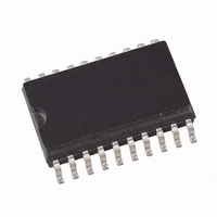
IC RCVR ASK/FSK UHF 20-SSOP
Manufacturer
Atmel
Datasheet
1.ATA5723-DK.pdf
(46 pages)
Specifications of ATA5724P3-TKQY
Frequency
433MHz
Sensitivity
-113dBm
Data Rate - Maximum
10 kbps
Modulation Or Protocol
ASK, FSK
Applications
General Purpose
Current - Receiving
11mA
Data Interface
PCB, Surface Mount
Antenna Connector
PCB, Surface Mount
Voltage - Supply
4.5 V ~ 5.5 V
Operating Temperature
-40°C ~ 125°C
Package / Case
20-SOIC (0.200", 5.30mm Width)
Operating Temperature (min)
-40C
Operating Temperature (max)
105C
Operating Temperature Classification
Industrial
Product Depth (mm)
4.4mm
Operating Supply Voltage (min)
4.5V
Operating Supply Voltage (typ)
5V
Operating Supply Voltage (max)
5.5V
Lead Free Status / RoHS Status
Lead free / RoHS Compliant
Features
-
Memory Size
-
Lead Free Status / Rohs Status
Compliant
Available stocks
Company
Part Number
Manufacturer
Quantity
Price
Part Number:
ATA5724P3-TKQY
Manufacturer:
ATMEL/爱特梅尔
Quantity:
20 000
6. Polling Circuit and Control Logic
7. Basic Clock Cycle of the Digital Circuitry
10
ATA5723/ATA5724/ATA5728
The receiver is designed to consume less than 1 mA while being sensitive to signals from a cor-
responding transmitter. This is achieved using the polling circuit. This circuit enables the signal
path periodically for a short time. During this time the bit-check logic verifies the presence of a
valid transmitter signal. Only if a valid signal is detected, the receiver remains active and trans-
fers the data to the connected microcontroller. If there is no valid signal present, the receiver is
in sleep mode most of the time resulting in low current consumption. This condition is called poll-
ing mode. A connected microcontroller is disabled during that time.
All relevant parameters of the polling logic can be configured by the connected microcontroller.
This flexibility enables the user to meet the specifications in terms of current consumption, sys-
tem response time, data rate etc.
The receiver is very flexible with regards to the number of connection wires to the microcon-
troller. It can be either operated by a single bi-directional line to save ports to the connected
microcontroller or it can be operated by up to five uni-directional ports.
The complete timing of the digital circuitry and the analog filtering is derived from one clock. This
clock cycle T
30 circuit. According to
tor (f
the local oscillator (f
T
basic clock cycle is T
T
Most applications are dominated by three transmission frequencies: f
used in USA, f
the aforementioned frequencies, T
For calculation of T
“Electrical Characteristics ATA5724, ATA5728” on page
Clk
Clk
• Timing of the polling circuit including bit check
• Timing of the analog and digital signal processing
• Timing of the register programming
• Frequency of the reset marker
• IF filter center frequency (fIF0)
• Application 315 MHz band (f
• Application 868.3 MHz band (f
• Application 433.92 MHz band (f
= 2.066 µs for f
controls the following application-relevant parameters:
XTO
) is defined by the RF input signal (f
Clk
Transmit
is derived from the crystal oscillator (XTO) in combination with a divide by 28 or
RF
Clk
LO
Clk
= 868.3 MHz and 433.92 MHz in Europe. All timings are based on T
= 868.3 MHz and T
). The basic clock cycle for ATA5724 and ATA5728 is T
for applications using other frequency bands, see table in
Section 3. “RF Front-end” on page
= 30/f
REF
XTO
giving T
XTO
Clk
XTO
= 14.71875 MHz, f
is given as:
= 13.55234 MHz, f
= 13.52875 MHz, f
Clk
Clk
= 2.0382 µs for f
RFin
= 2.069 µs for f
) which also defines the operating frequency of
LO
LO
37.
= 314.13 MHz, T
LO
5, the frequency of the crystal oscilla-
= 867.35 MHz, T
= 432.93 MHz, T
RF
RF
= 433.92 MHz. For ATA5723 the
= 315 MHz.
Transmit
Clk
Clk
= 315 MHz is mainly
= 2.0382 µs)
Clk
= 2.066 µs)
Clk
= 2.0696 µs)
28/f
9106E–RKE–07/08
Section 18.
XTO
Clk
giving
. For


