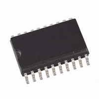
ATA5724P3-TKQY Atmel, ATA5724P3-TKQY Datasheet - Page 13

ATA5724P3-TKQY
Manufacturer Part Number
ATA5724P3-TKQY
Description
IC RCVR ASK/FSK UHF 20-SSOP
Manufacturer
Atmel
Datasheet
1.ATA5723-DK.pdf
(46 pages)
Specifications of ATA5724P3-TKQY
Frequency
433MHz
Sensitivity
-113dBm
Data Rate - Maximum
10 kbps
Modulation Or Protocol
ASK, FSK
Applications
General Purpose
Current - Receiving
11mA
Data Interface
PCB, Surface Mount
Antenna Connector
PCB, Surface Mount
Voltage - Supply
4.5 V ~ 5.5 V
Operating Temperature
-40°C ~ 125°C
Package / Case
20-SOIC (0.200", 5.30mm Width)
Operating Temperature (min)
-40C
Operating Temperature (max)
105C
Operating Temperature Classification
Industrial
Product Depth (mm)
4.4mm
Operating Supply Voltage (min)
4.5V
Operating Supply Voltage (typ)
5V
Operating Supply Voltage (max)
5.5V
Lead Free Status / RoHS Status
Lead free / RoHS Compliant
Features
-
Memory Size
-
Lead Free Status / Rohs Status
Compliant
Available stocks
Company
Part Number
Manufacturer
Quantity
Price
Part Number:
ATA5724P3-TKQY
Manufacturer:
ATMEL/爱特梅尔
Quantity:
20 000
8.2
8.3
Figure 8-2.
9106E–RKE–07/08
Data_out (DATA)
Bit-check Mode
Configuring the Bit Check
IC_ACTIVE
(Number of checked Bits: 3)
Bit check
Dem_out
Timing Diagram for Complete Successful Bit Check
Start-up mode
In bit-check mode the incoming data stream is examined to distinguish between a valid signal
from a corresponding transmitter and signals due to noise. This is done by subsequent time
frame checks where the distances between 2 signal edges are continuously compared to a pro-
grammable time window. The maximum number of these edge-to-edge tests, before the
receiver switches to receiving mode, is also programmable.
Assuming a modulation scheme that contains two edges per bit, two time frame checks verify
one bit. This is valid for Manchester, Bi-phase, and most other modulation schemes. The maxi-
mum count of bits to be checked can be set to 0, 3, 6, or 9 bits using the variable N
OPMODE register. This implies 0, 6, 12, and 18 edge-to-edge checks respectively. If N
set to a higher value, the receiver is less likely to switch to receiving mode due to noise. In the
presence of a valid transmitter signal, the bit check takes less time if N
value. In polling mode, the bit-check time is not dependent on NBit-check.
example where three bits are tested successfully and the data signal is transferred to pin DATA.
According to
If the edge-to-edge time t
bit-check limit T
the bit check is terminated and the receiver switches to sleep mode.
Figure 8-3.
T
Start-up
Figure
Valid Time Window for Bit Check
Lim_max
8-3, the time window for the bit check is defined by two separate time limits.
Dem_out
, the check continues. If t
1/2 Bit
ee
1/2 Bit
is in between the lower bit-check limit T
Start-check mode
T
Bit-check
1/2 Bit
T
T
Lim_max
Lim_min
ATA5723/ATA5724/ATA5728
Bit check ok
t
ee
1/2 Bit
ee
is smaller than T
1/f
Sig
1/2 Bit
1/2 Bit
Lim_min
Receiving mode
Bit-check
or t
Lim_min
Figure 8-2
ee
exceeds T
is set to a lower
and the upper
Bit-check
shows an
Bit-check
Lim_max
in the
13
is
,


