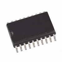
ATA5724P3-TKQY Atmel, ATA5724P3-TKQY Datasheet - Page 14

ATA5724P3-TKQY
Manufacturer Part Number
ATA5724P3-TKQY
Description
IC RCVR ASK/FSK UHF 20-SSOP
Manufacturer
Atmel
Datasheet
1.ATA5723-DK.pdf
(46 pages)
Specifications of ATA5724P3-TKQY
Frequency
433MHz
Sensitivity
-113dBm
Data Rate - Maximum
10 kbps
Modulation Or Protocol
ASK, FSK
Applications
General Purpose
Current - Receiving
11mA
Data Interface
PCB, Surface Mount
Antenna Connector
PCB, Surface Mount
Voltage - Supply
4.5 V ~ 5.5 V
Operating Temperature
-40°C ~ 125°C
Package / Case
20-SOIC (0.200", 5.30mm Width)
Operating Temperature (min)
-40C
Operating Temperature (max)
105C
Operating Temperature Classification
Industrial
Product Depth (mm)
4.4mm
Operating Supply Voltage (min)
4.5V
Operating Supply Voltage (typ)
5V
Operating Supply Voltage (max)
5.5V
Lead Free Status / RoHS Status
Lead free / RoHS Compliant
Features
-
Memory Size
-
Lead Free Status / Rohs Status
Compliant
Available stocks
Company
Part Number
Manufacturer
Quantity
Price
Part Number:
ATA5724P3-TKQY
Manufacturer:
ATMEL/爱特梅尔
Quantity:
20 000
Figure 8-4.
14
(Lim_min = 14, Lim_max = 24)
IC_ACTIVE
Bit-check
Bit check
Dem_out
counter
ATA5723/ATA5724/ATA5728
Timing Diagram During Bit Check
Start-up mode
T
Start-up
For best noise immunity using a low span between T
achieved using a fixed frequency at a 50% duty cycle for the transmitter preburst. A “11111...” or
a “10101...” sequence in Manchester or Bi-phase is suitable for this. A good compromise
between receiver sensitivity and susceptibility to noise is a time window of ±30% regarding the
expected edge-to-edge time t
periods, the bit-check limits must be programmed according to the required span.
The bit-check limits are determined by means of the formula below.
T
T
Lim_min and Lim_max are defined by a 5-bit word each within the LIMIT register.
Using above formulas, Lim_min and Lim_max can be determined according to the required
T
mum edge-to-edge time t
“Digital Signal Processing” on page
imum value of the upper limit is Lim_max = 63.
If the calculated value for Lim_min is < 19, it is recommended to check 6 or 9 bits (N
prevent switching to receiving mode due to noise.
Figure
Lim_min = 14 and Lim_max = 24. When the IC is enabled, the signal processing circuits are
enabled during T
that period. When the bit check becomes active, the bit-check counter is clocked with the cycle
T
Figure 8-4
limits defined by Lim_min and Lim_max at the occurrence of a signal edge. In
check fails as the value CV_Lim is lower than the limit Lim_min. The bit check also fails if
CV_Lim reaches Lim_max. This is illustrated in
0
Lim_min
Lim_max
Lim_min
XClk
.
, T
= Lim_min
8-4,
1 2
= (Lim_max – 1)
Lim_max
shows how the bit check proceeds if the bit-check counter value CV_Lim is within the
3 4
Figure
T
5 6
XClk
Startup
and T
7 8
T
8-5, and
. The output of the ASK/FSK demodulator (Dem_out) is undefined during
1 2
XClk
XClk
3 4
. The time resolution defining T
ee
T
XClk
ee
(t
5 6
DATA_L_min
. Using pre-burst patterns that contain various edge-to-edge time
Figure 8-6
7 8
1/2 Bit
16. The lower limit should be set to Lim_min
9 10
Bit-check mode
11 12
, t
T
Bit-check
DATA_H_min
13 14
illustrate the bit check for the bit-check limits
Bit check ok
15 16
Figure
17 18
Lim_min
) is defined according to the
8-6.
1 2
Lim_min
3 4
and T
5 6
1/2 Bit
Lim_max
and T
7 8
9 10
Lim_max
is recommended. This is
11 12
Bit check ok
13 14
is T
Figure 8-5
15
XClk
1 2
1/2 Bit
9106E–RKE–07/08
10. The max-
Section 8.6
. The mini-
3 4
Bit-check
the bit
) to


