JN5139-Z01-V NXP Semiconductors, JN5139-Z01-V Datasheet
JN5139-Z01-V
Specifications of JN5139-Z01-V
935293943515
JN5139-Z01-AI
JN5139-Z01-V
JN5139-Z01R1-ARV
JN5139-Z01R1V


Related parts for JN5139-Z01-V


JN5139-Z01-V Summary of contents
Page 1
... Data Sheet: JN5139-001 and JN5139-Z01 IEEE802.15.4 and ZigBee Wireless Microcontrollers Overview The JN5139 is a low power, low cost wireless microcontroller suitable for IEEE802.15.4 and ZigBee applications. RISC processor, with a fully compliant 2.4GHz IEEE802.15.4 transceiver, 192kB of ROM, 96kB of RAM, and a rich mixture of analogue and digital peripherals ...
Page 2
... External Reset 6.3 Software Reset 7 Interrupt System 7.1 System Calls 7.2 Processor Exceptions 7.2.1 Bus Error 7.2.2 Alignment 7.2.3 Illegal Instruction 7.3 Hardware Interrupts 8 Wireless Transceiver 8.1 Radio 8.1.1 Radio External components 8.1.2 Antenna Diversity 8.2 Modem 8.3 Baseband Processor 2 JN-DS-JN5139 1v9 ...
Page 3
... Security 8.4 Security Coprocessor 9 Digital Input/Output 10 Serial Peripheral Interface 11 Intelligent Peripheral Interface 11.1 Data Transfer Format 11.2 JN5139 (Slave) Initiated Data Transfer 11.3 Remote Processor (Master) Initiated Data Transfer 12 Timers 12.1 Peripheral Timer / Counters 12.1.1 Pulse Width Modulation Mode 12.1.2 Capture Mode 12 ...
Page 4
... B.1.1 Crystal Equivalent Circuit B.1.2 Crystal Load Capacitance B.1.3 Crystal ESR and Required Transconductance B.2 16MHz Oscillator B.3 Applications Information B.3.1 Typical Application Schematic B.3.2 Reference Designs Appendix C Related Documents RoHS Compliance Status Information Disclaimers Version Control Contact Details 4 JN-DS-JN5139 1v9 ...
Page 5
... A 32-bit RISC CPU allows software to be run on-chip, its processing power being shared between the IEEE802.15.4 MAC protocol, other higher layer protocols and the user application. The JN5139 has a unified memory architecture, code memory, data memory, peripheral devices and I/O ports are organized within the same linear address space. ...
Page 6
... Slave SPI port (shared with digital I/O) • Twenty-one digital I/O lines (multiplexed with UARTs, timers and SPI selects) • Four-channel, 12-bit, Analogue-to-Digital converter • Two 11-bit Digital-to-Analogue converters • Two programmable analogue comparators • Internal temperature sensor and battery monitor JN-DS-JN5139 1v9 © NXP Laboratories UK 2010 ...
Page 7
... UART1 1.8V Timer0 Timer1 32kHz Osc 2-Wire Serial Interface Intelligent Peripheral Wireless Transceiver Security Coprocessor Baseband Controller Modem Radio Figure 1: JN5139 Block Diagram JN-DS-JN5139 1v9 SPICLK SPIMOSI SPIMISO SPISEL0 DIO0/SPISEL1 DIO1/SPISEL2 DIO2/SPISEL3/RFRX DIO3/SPISEL4/RFTX DIO4/CTS0 DIO5/RTS0 DIO6/TXD0 DIO7/RXD0 DIO17/CTS1/IP_SEL DIO18/RTS1/IP_INT DIO19/TXD1 DIO20/RXD1 M ...
Page 8
... RESETN 8 VSS3 9 VSSS 10 XTALOUT 11 XTALIN 12 VB_SYN 13 VCOTUNE 14 Figure 2: 56-pin QFN Configuration (top view) Note: Please refer to Appendix B.3 for important applications information regarding the connection of the PADDLE to the PCB. 8 PADDLE JN-DS-JN5139 1v9 42 DIO2/SPISEL3/RFRX 41 DIO1/SPISEL2 40 VB_MEM 39 VSS1 38 DIO0/SPISEL1 37 SPISEL0 36 SPIMOSI 35 VB_DIG1 34 SPIMISO ...
Page 9
... DIO15 or Serial Interface Data or Intelligent Peripheral Data Out DIO16 or Intelligent Peripheral Data In DIO17 or UART 1 Clear To Send Input or Intelligent Peripheral Device Select Input DIO18 or UART 1 Request To Send Output or Intelligent Peripheral Interrupt Output DIO19 or UART 1 Transmit Data Output DIO20 or UART 1 Receive Data Input JN-DS-JN5139 1v9 9 ...
Page 10
... RESETN is a bi-directional active low reset pin that is connected to a 40kΩ internal pull-up resistor. It may be pulled low by an external circuit, or can be driven low by the JN5139 if an internal reset is generated. Typically, it will be used to provide a system reset signal. Refer to section 6.2, External Reset, for more details. ...
Page 11
... Peripheral 2.2.6 Digital Input/Output Digital I/O pins on the JN5139 can have signals applied higher than VDD2 (with the exception of pins DIO9 and DIO10 that are 3V tolerant) and are therefore TTL-compatible with VDD2 > 3V. For other DC properties of these pins see section 17.2.3 I/O Characteristics. ...
Page 12
... GP registers to contain the address of objects. Subroutine parameter passing is also made more efficient by using GP registers rather than pushing objects on the stack. The recommended programming method for the JN5139 is by using C, which is supported by a software developer kit comprising a C compiler, linker and debugger. ...
Page 13
... Memory Organisation This section describes the different memories found within the JN5139. The device contains ROM, RAM, OTP eFuse memory, the wireless transceiver and peripherals all within the same linear address space. © NXP Laboratories UK 2010 0xFFFFFFFF RAM 0xF0018000 RAM (96kB) ...
Page 14
... RAM The JN5139 contains 96k bytes of high speed RAM organized as 24k x 32-bit. It can be used for both code and data storage and is accessed by the CPU in a single clock cycle. At reset, a boot loader controls the loading of segments of code and data from an external memory connected to the SPI port, into RAM. Software can control the power supply to the RAM allowing the contents to be maintained during a sleep period when other parts of the device are un-powered ...
Page 15
... OTP eFuse Memory The JN5139 contains 48-bytes of eFuse memory; this is one time programmable memory that is organised 32-bit words, 4 words are reserved by Jennic and 4 words are reserved for future use. The remaining 4 words are fully user programmable, designed to allow for the storage of a 128-bit encryption key for secure external memory encryption (see section 4 ...
Page 16
... When bootloading program code from external serial memory, the JN5139 automatically accesses the encryption key to execute the decryption process. User program code does not need to handle any of the decryption process transparent process. With encryption enabled, the time taken to boot code from external Flash memory is increased. ...
Page 17
... System Clocks Two system clocks are used to provide timing references into the on-chip subsystems of the JN5139. A 16MHz clock, generated by a crystal-controlled 16MHz oscillator, is used by the transceiver, processor, memory and digital and analogue peripherals. A 32kHz clock is used by the sleep timer and during the startup phase of the chip. ...
Page 18
... External Clock An externally supplied 32kHz reference clock on the CLK32K input (DIO9) may be provided to the JN5139. This would allow the 32kHz system clock to be sourced from a very stable external oscillator module, allowing more accurate sleep cycle timings. (See section 17.2.3 I/O Characteristics, DIO9 tolerant input) ...
Page 19
... A system reset initialises the device to a predefined state and forces the CPU to start program execution from the reset vector. The reset process that the JN5139 goes through is as follows. When power is applied, the internal 32kHz oscillator starts up and stabilises, which takes approximately 100μsec. At this point, the 16MHz crystal oscillator is enabled and power is applied to the processor and digital logic ...
Page 20
... RESETN pin is driven low for 1µsec; depending on the external components this may or may not be visible on the pin. In addition, the RESETN line can be driven low by the JN5139 to provide a reset to other devices in the system (e.g. external sensors) without resetting itself. When the RESETN line is not driven it will pull back high through either the internal pull-up resistor or any external circuitry essential to ensure that the RESETN line pulls back high within 100µ ...
Page 21
... Interrupt System The interrupt system on the JN5139 is a hardware-vectored interrupt system. The JN5139 provides several interrupt sources, some associated with CPU operations (CPU exceptions) and others which are used by hardware in the device. When an interrupt occurs the CPU stops executing the current program and loads its program counter with a fixed hardware address specific to that interrupt ...
Page 22
... Further details of interrupts are provided for the functions in their respective sections in this datasheet. Interrupts are used to wake the JN5139 from sleep. The peripherals, baseband controller, security coprocessor and PIC are powered down during sleep but the DIO interrupts and optionally the wake-up timers and analogue comparator interrupts remain powered to bring the JN5139 out of sleep ...
Page 23
... PA drives the antenna via the RX/TX switch. © NXP Laboratories UK 2010 VGA PA (I) LOI Trim LOQ VGA PA (Q) Trim Calibration VGA1 VGA2 VCO PLL Calibration Figure 14: Radio Architecture JN-DS-JN5139 1v9 IDATA DAC QDATA DAC IF DATA ADC AGC Reference & BIAS 23 ...
Page 24
... So packet is transmitted and no acknowledgement is received, the radio system can switch to the other antenna for the retry, with a different probability of success. The JN5139 provides an output on DIO12 that is asserted on odd numbered retries that can be used to control an antenna switch; this enables antenna diversity to be implemented easily (see Figure 16 and Figure 17) ...
Page 25
... The demodulator performs digital IF down-conversion and matched filtering and is extremely tolerant to carrier frequency offsets in excess of ±80ppm without suffering any significant degradation in performance. © NXP Laboratories UK 2010 TX-RX Cycle st RX O-QPSK Detection Demodulation (Despreading O-QPSK Spreading Modulation Q Q Figure 18: Modem Architecture JN-DS-JN5139 1v9 2 TX-RX Cycle (1 Retry Symbol RX Data Interface TX Data Interface 25 ...
Page 26
... Modem. At the same time, the radio is prepared 26 Encrypt Port AES AES Codec Codec Inline Security Backoff Control Decrypt Port Figure 19: Baseband Processor JN-DS-JN5139 1v9 Tx/Rx Frame Buffer Protocol Timers Processor Bus © NXP Laboratories UK 2010 ...
Page 27
... As well as being used during in-line encryption/decryption operations over a streaming interface and in external memory encryption also possible to use the AES core as a coprocessor to the CPU of the JN5139. To allow the hardware to be shared between the two interfaces an arbiter ensures that the streaming interface to the AES core always has priority, to ensure that in-line processing can take place at any time ...
Page 28
... Information such as the type of security operation to be performed and the encrypt/decrypt key to be used must also be provided. Processor Interface In-line Interface Figure 20: Security Coprocessor Architecture 28 AES Block AES Encrpytion Encoder Controller JN-DS-JN5139 1v9 © NXP Laboratories UK 2010 ...
Page 29
... NXP Laboratories UK 2010 SPICLK, MOSI, MISO SPISEL<4:0> TxD RxD RTS CTS TxD RxD RTS CTS TIM0CK_GT TIM0CAP TIM0OUT TIM1CK_GT TIM1CAP TIM1OUT SIF_CLK SIF_D IP_CLK IP_DI IP_DO IP_SEL IP_INT RFTX DIO<20:0> Figure 21: DIO Block Diagram JN-DS-JN5139 1v9 SPISEL<0> DIO<20:0> MUX Chip Pins 29 ...
Page 30
... After wake-up the DIO will still be an output with the same value but controlled from the GPIO Data/Direction registers. It can be altered with the software functions that adjust the DIO, or the application may re-configure SPISEL1. Unused DIO pins are recommended to be set as inputs with the pull-up enabled. 30 JN-DS-JN5139 1v9 © NXP Laboratories UK 2010 ...
Page 31
... The Serial Peripheral Interface (SPI) allows high-speed synchronous data transfer between the JN5139 and peripheral devices. The JN5139 operates as a master on the SPI bus and all other devices connected to the SPI are expected to be slave devices under the control of the JN5139 CPU. The SPI includes the following features: • ...
Page 32
... The clock polarity controls if SCLK is high or low between transfers (and hence the polarity of the first clock edge in a transfer). The clock phase and polarity determines which edge of SPICLK is used by the JN5139 to present new data on the SPIMOSI line; the opposite edge will be used to read data from the SPIMISO line. The interface should be configured appropriately for the SPI slave being accessed ...
Page 33
... An interrupt can be generated when the transaction has completed or alternatively the interface can be polled slave device wishes to signal the JN5139 indicating that it has data to provide, it may be connected to one of the DIO pins that can be enabled as an interrupt. ...
Page 34
... The first byte transferred into the JN5139 is a status byte with the format shown in Table 4. This is followed by a padding byte that should be set to zero. The first byte output by the JN5139 is a padding byte, that should be ignored, followed by a status byte with the format shown in Table 4 ...
Page 35
... IP_DI with RXRDY set. After receiving the status byte from the JN5139, it should check that the JN5139 has a buffer ready by reading the TXRDY bit of the received status byte. If the TXRDY bit is 0, indicating that the JN5139 does not have data to send, it must terminate the transfer by deasserting IP_SEL unless it is transmitting data to the JN5139 ...
Page 36
... Interrupt Generator Rise = Fall = Delta-Sigma PWM/Δ−Σ Counter PWM/Δ−Σ Reset System Single Reset Shot Figure 26: Timer Unit Block Diagram prescale JN-DS-JN5139 1v9 OE S TIMxOUT R PW M/Delta- Sigma value. For example, a prescale value © NXP Laboratories UK 2010 ...
Page 37
... Therefore, if multiple pulses are seen on TIMxCAP before the counter is stopped only the last pulse width will be stored. CLK CAPT Rise Fall © NXP Laboratories UK 2010 Rise Fall Figure 27: PWM Output Timings RISE RISE Capture Mode Enabled Figure 28: Capture Mode JN-DS-JN5139 1v9 FALL ...
Page 38
... RTZ and NRZ for the same programmed number of pulses Conversion cycle 1 Figure 29: Return To Zero Mode in Operation clocks. The integrated output will only reach half VDD2 in RTZ mode Conversion cycle Conversion cycle 1 Conversion cycle Figure 30: Non-Return to Zero Mode JN-DS-JN5139 1v9 © NXP Laboratories UK 2010 ...
Page 39
... Timer / Counter Application Figure 31 shows an application of the JN5139 timers to provide closed loop speed control. Timer 0 is configured in PWM mode to provide a variable mark-space ratio switching waveform to the gate of the NFET. This in turn controls the power in the DC motor. Timer 1 is configured to count the rising edge events on the clk/gate pin over a constant period. This converts the tacho pulse stream output into a count proportional to the motor speed ...
Page 40
... Tick Timer The JN5139 contains a hardware timer that can be used for generating timing interrupts to software. It may be used to implement regular events such as ticks for software timers or an operating system high-precision timing reference or can be used to implement system monitor timeouts as used in a watchdog timer. Features include: • ...
Page 41
... A calibration reference timer, clocked from the crystal oscillator, is provided to allow comparisons to be made between the RC clock and the 16MHz crystal oscillator when the JN5139 is awake. Operation is as follows: • ...
Page 42
... Serial Communications The JN5139 has two independent Universal Asynchronous Receiver / Transmitter (UART) serial communication interfaces. These provide similar operating features to the industry standard 16550A device operating in FIFO mode. Each interface performs serial-to-parallel conversion on incoming serial data and parallel-to-serial conversion on outgoing data from the CPU to external devices. In both directions, a 16-byte deep FIFO buffer allows the CPU to read and write multiple characters on each transaction ...
Page 43
... The following example shows the UART connected to a 9-pin connector compatible with a PC. The software developer kit uses such an interface as the debugger interface between the JN5139 and a PC. As the JN5139 device pins do not provide the RS232 line voltage a level shifter is used. ...
Page 44
... Two-Wire Serial interface The JN5139 includes an industry standard two-wire synchronous serial interface (SIF) that provides a simple and efficient method of data exchange between devices. The system operates as a master only and uses a serial data line (SIF_D) and a serial clock line (SIF_CLK) to perform bi-directional data transfers; includes the following features: 2 • ...
Page 45
... The first byte of data transferred by the device after a start bit is the slave address. The JN5139 supports both 7-bit and 10-bit slave addresses by generating either one or two address transfers. Only the slave with a matching address will respond by returning an acknowledge bit. 14.1 Connecting Devices The clock and data lines, SIF_D and SIF_CLK, are alternative functions of DIO lines 15 and 14 respectively ...
Page 46
... Analogue Peripherals The JN5139 contains a number of analogue peripherals allowing the direct connection of a wide range of external sensors, switches and actuators. Chip Boundary VREF ADC1 ADC2 ADC3 ADC4 Temp Sensor COMP1P COMP1M COMP2P COMP2M DAC1 DAC2 Figure 38: On-chip Analogue Peripherals In order to provide good isolation from digital noise, the analogue peripherals are powered by a separate regulator, supplied from the analogue supply VDD1 and referenced to analogue ground VSSA ...
Page 47
... Polling over this period would be wasteful of processor bandwidth. © NXP Laboratories UK 2010 Maximum Input Range Supply Voltage Range (VDD) 1.2V 1.6V 2.4V 3.2V Sample Switch Figure 39 ADC Input Equivalent Circuit JN-DS-JN5139 1v9 2.2V - 3.6V 2.2V - 3.6V 2.6V - 3.6V 3.4V - 3.6V ADC front end 47 ...
Page 48
... Conversion on either channel can then be performed by disabling the unused channel and enabling the channel to be updated. The DACs should not be used in single shot mode, but continuous conversion mode only, in order to maintain a steady output voltage. 48 JN-DS-JN5139 1v9 © NXP Laboratories UK 2010 ...
Page 49
... This mode may be used during non-sleep operation however it is particularly useful in sleep mode to wake up the JN5139 from sleep where low current consumption is important. The wakeup action and the configuration for which edge of the comparator output will be active are controlled through software. In sleep mode the negative input signal source, must be configured to be driven from the external pins. © ...
Page 50
... The current consumption figures for the different modes of operation of the device is given in section 17.2.2. 16.2 Active Processing Mode Active processing mode in the JN5139 is where all of the application processing takes place. All of the peripherals are available to the application as are options to actively enable or disable them to control power consumption; see specific peripheral sections for details. To further reduce power consumption, there is also the option to doze the CPU but keep the rest of the chip active ...
Page 51
... The comparator can generate a wakeup interrupt when a change in the relative levels of the positive and negative inputs occurs. The ability to wakeup when continuously monitoring analogue signals is useful in ultra-low power applications. For example, the JN5139 can remain in sleep mode until the voltage drops below a threshold and then be woken up to deal with the alarm condition. ...
Page 52
... VDD1, VDD2 Ambient temperature range 52 Min -0.3V -0.3V -0.3V -0.3V -0.3V -0.3V -40º Min 2.2V -40ºC JN-DS-JN5139 1v9 Max 3.6V 1.98V VB_xxx + 0.3V VDD1 + 0.3V Lower of (VDD2 + 2V) and 5.5V VDD2 + 0.3V 150ºC 260ºC 2.0kV 200V 500V Max 3.6V 85ºC ...
Page 53
... Typ Max Unit 60 250 nA JN-DS-JN5139 1v9 Notes SPI, DIOs enabled, code executing in RAM (see 16.2) CPU in software doze – radio transmitting CPU in software doze – radio in receive mode Temperature sensor and battery measurements require ADC One / both ...
Page 54
... RISE V POT VDD t STAB Figure 40: Power-on Reset t RST V RST t STAB Figure 41: External Reset JN-DS-JN5139 1v9 Unit Notes VDD2 = 3.6V kΩ VDD2 = 3.0V VDD2 = 2. Tolerant I/O only With 4mA load V With 4mA load V With 3mA load V With 3mA load mA VDD2 = 2.7V to 3.6V VDD2 = 2 ...
Page 55
... VO Figure 42: SPI Timing (Master) Min 62.5 15.3 @ 2.7-3.6V 30.5 @ 2.2-3. (SPICLK = 16MHz) 0 (SPICLK<16MHz, mode (SPICLK<16MHz, mode JN-DS-JN5139 1v9 Unit Notes Assumes internal pullup µs resistor value of 100K worst case and ~5pF external capacitance V Minimum voltage to avoid being reset V VDD2 = 2.2V VDD2 = 3 ...
Page 56
... R SU;DAT HD;STA SU;STA t HIGH Standard Mode Symbol Min f 0 SCL t 4 HD:STA t 4.7 LOW JN-DS-JN5139 1v9 t ssh t hz Max Unit - BUF t SU;STO Fast Mode Unit Max Min Max 100 0 400 kHz - 0.6 - µs - 1.3 - µs © NXP Laboratories UK 2010 ...
Page 57
... SU:STO t 4.7 - BUF C - 400 b V 0.1VDD - nl V 0.2VDD - nh Typ Max 2.75 + 0.5* program size in kBytes 2.75 + 0.5* program size in kBytes 2.75 0.2 JN-DS-JN5139 1v9 0.6 - µs 0.5 - µs 0.1 - µs 20+0.1Cb 300 ns 20+0.1Cb 300 ns 0.6 - µs 1.3 - µs - 400 pF 0.1VDD - V 0.2VDD ...
Page 58
... JN-DS-JN5139 1v9 Notes 3.6V 3.0V 2.2V Typical at 3.0V 25°C For a 1 second sleep period calibrating over 20 x 32kHz clock periods Notes Including bandgap ref. Assuming xtal with ESR of 40ohms and CL= 9pF External caps = 15pF ...
Page 59
... Typ Max 12 655 ± +10 -20 500 Vref or 2*Vref See Section 17.3.8 Bandgap Reference 1.2 1.6 8 JN-DS-JN5139 1v9 Unit Notes 25ºC ppm/° 85ºC -40ºC to 0ºC ºC Unit Notes bits 500kHz Clock µA LSB 0 to Vref range LSB Guaranteed monotonic mV ...
Page 60
... Lower of Vdd-1.2 and Vref 0 Lower of 2x(Vdd-1.2 ) and Vdd-0.2 and 2xVref See Section 17.3.8 Bandgap Reference 0.8 1.2 1 Binary JN-DS-JN5139 1v9 Unit Notes bits µA LSB LSB Guaranteed monotonic mV mV 16MHz input clock, programmable prescaler µs With 10k ohms & 20pF load µ ...
Page 61
... Radio Transceiver The JN5139 meets all the requirements of the IEEE802.15.4 standard for 2.2-3.6V and offers the following improved RF characteristics. All RF characteristics are measured single ended and include the losses of a ceramic balun. This part also meets the following regulatory body approvals, when used with Jennic’s Module Reference Designs. ...
Page 62
... Transmitter Characteristics +1.5 dBm +2.7 dBm -31 five 6dB steps (Note2) dBm Measured conducted into 50ohms -66 -63 30MHz to 1GHz, -41 -38 1GHz to12.5GHz, The following exceptions apply 1.8 to 1.9GHz & 5.15 to 5.3GHz -72 JN-DS-JN5139 1v9 Notes © NXP Laboratories UK 2010 ...
Page 63
... Modulated Interferers at 2 & 4 channel separation (Note1 -95 to -10dBm Transmitter Characteristics +2 dBm +3 dBm -31 five 6dB steps (Note2) dBm Measured conducted into 50ohms 30MHz to 1GHz, -64 -61 1GHz to12.5GHz, -38 -35 The following exceptions apply 1.8 to 1.9GHz & 5.15 to 5.3GHz -72 JN-DS-JN5139 1v9 Notes Notes 63 ...
Page 64
... JN-DS-JN5139 1v9 Notes Notes Nominal for 1% PER, as per 802.15.4 section 6.5.3.3 For 1% PER, measured as sensitivity For 1% PER with wanted signal 3dB above sensitivity, (Note1) For 1% PER with wanted signal 3dB above sensitivity, (Note1) ...
Page 65
... Note2 extra 4dB of attenuation is available if required. © NXP Laboratories UK 2010 Typical Max Unit -72 12 [3. -38 -20 dBc JN-DS-JN5139 1v9 Notes The following exceptions apply 1.8 to 1.9GHz & 5.15 to 5.3GHz At maximum output power At greater than 3.5MHz offset, as per 802.15.4, section 6.5.3.1 65 ...
Page 66
... Appendix A Mechanical and Ordering Information A.1 56pin QFN Package Drawing 66 JN-DS-JN5139 1v9 Controlling Dimension: mm millimetres Symbol Min. Nom. Max. A ------ ------ 0.9 A1 0.00 0.01 0.05 A2 ------ 0.65 0.7 A3 0.20 Ref. b 0.2 0.25 0.3 D 8.00 bsc D1 7.75 bsc D2 6.20 6.40 6.60 E 8.00 bsc E1 7.75 bsc E2 6 ...
Page 67
... A.2 PCB Decal The following PCB decal is recommended; all dimensions are in millimetres (mm). For further detail please consult the Module Development Reference Manual JN-RM-2006, available to download from the Jennic Support web site (www.nxp.com/jennic/support) © NXP Laboratories UK 2010 JN-DS-JN5139 1v9 67 ...
Page 68
... A.3 Ordering Information The standard qualification for the JN5139 is Industrial Specification: -40ºC to +85ºC, packaged in a 56-pin QFN (Quad Flat No-leads) package. Ordering Code Format: JN5139/XXX ROM Variant XXX: 001 IEEE802.15.4 Z01 ZigBee Ordering Codes: Part Number Ordering Code JN5139-001 JN5139/001 ...
Page 69
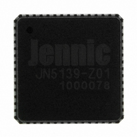
... A.4 Device Package Marking The diagram below shows the package markings for JN5139 devices. The package on the left along with the legend information below it, shows the general format of package marking. The package on the right shows the specific markings for a JN5139-001 device, that came from assembly build number 1000004 and was manufactured week 4 of 2007 ...
Page 70
... Figure 46 shows the detailed dimensions of the tape used for 8x8mm 56QFN devices. 70 Figure 45: Tape and Reel Orientation Reference Dimensions (mm) 8.30 ±0. 8.30 ±0. 1.10 ±0. 12.00 ±0.10 P 0.30 ±0. 16.00 +0.30/-0.10 Figure 46: Tape Dimensions JN-DS-JN5139 1v9 © NXP Laboratories UK 2010 ...
Page 71
... All dimensions and tolerances are fully compliant with EIA-481-B and are specified in millimetres. 6 window design with one window on each side blanked to allow adequate labelling space. Tape Width A B (min) 16 180 1.5min © NXP Laboratories UK 2010 9 11 – 10e Ohms Square (min) 13 ±0.2 60 +0.1 –0.0 Figure 47: Reel Dimensions JN-DS-JN5139 1v9 W (max) 16.40 17.90 71 ...
Page 72
... MIL-L-8835 specification. The MBB has a moisture-sensitivity caution label to indicate the moisture-sensitive classification of the enclosed devices – 10e Ohms Square C D (min) N (min) 13 +0.5 -0.2 20.2 100 JN-DS-JN5139 1v9 W (min) W (max) 15.90 19.40 © NXP Laboratories UK 2010 ...
Page 73
... PCB and land pattern designs are key to board level reliability, and Jennic strongly recommends that users follow the design rules listed in IPC-SM-782. For reflow profiles recommended to follow the reflow profile in Figure guide, as well as the paste manufacturers guidelines on peak flow temperature, soak times, time above liquidus and ramp rates. © NXP Laboratories UK 2010 Figure 48: Reflow Profile JN-DS-JN5139 1v9 73 ...
Page 74
... Load Capacitance 9pF and max ESR 40 Ω 15pF defines the oscillation frequency (series) m JN-DS-JN5139 1v9 Max Notes Including temperature and ageing See below for more 60Ω details See below for more details CL = 9pF, total external capacitance needs to be 2*CL. , allowing for stray ...
Page 75
... This gives C © NXP Laboratories UK 2010 × ⎛ ⎞ ˆ ⎜ ⎟ ⎜ ⎟ C ⎝ ⎠ NEG ω × × ⎛ ⎜ ≥ m ⎜ ω × × ⎝ JN-DS-JN5139 1v9 and C with C from the crystal ⎞ C ⎟ L ⎟ ⎠ ...
Page 76
... Crystal Oscillator Transconductance Versus Temperature 1.285 1.28 1.275 1.27 1.265 1.26 1.255 1.25 1.245 - ω × × =40Ω, C =1pF and =18pF ( for a load capacitance of 9pF), the 647uA/V. The JN5139 has a typical value for (VDD=3V) - Temperature (C) JN-DS-JN5139 1v9 × square law 100 © NXP Laboratories UK 2010 ...
Page 77
... B.2 16MHz Oscillator The JN5139 contains the necessary on-chip components to build a 16 MHz reference oscillator with the addition of an external crystal resonator, two tuning capacitors and a resistor. The schematic of these components are shown in Figure 49. The two capacitors, C1 and C2, will typically be 15pF ±5% and use a COG dielectric, R2 should be 1M5Ω. ...
Page 78
... R3 VB_SYN, VB_RF (See Schematic Notes Vcc Timers C13 UART 0 43 SPI S EL3 SPI S EL2 VB_M Jennic SPI S EL1 SPI S EL0 MOSI VB_DIG1 IC1: JN5139 MISO SPICL K COMP2M PADDLE COMP2P DAC2 DAC1 Printed Antenna Figure 50: Application Schematic Values 100nF 5% 15pF 5% (COG) 3n3F 5% 330pF 5% (COG) 4k7Ω ...
Page 79
... B.3.2 Reference Designs For customers wishing to integrate the JN5139 device directly into their system, Jennic provide a range of Module Reference Designs, covering standard and high-power modules fitted with different Antennae. These reference designs should be followed accurately to ensure the device operates as specified. For further detail please consult the Module Development Reference Manual JN-RM-2006, available to download from the Jennic Support web site (www.nxp.com/jennic/support) © ...
Page 80
... JN-AN-1038 Programming Flash devices not supported by the JN51xx ROM-based bootloader [5] JN-RM-2001 Integrated Peripherals API Reference Manual [6] JN-RM-2006 Module Development Reference Manual RoHS Compliance JN5139 devices meet the requirements of Directive 2002/95/EC of the European Parliament and of the Council on the Restriction of Hazardous Substance (RoHS). Status Information The status of this Data Sheet is Preliminary. ...
Page 81
... September 2008 – added min/max specifications, incorporated known errata 1.7 3rd April 2009 – Datasheet fully revised 1.8 15th May 2009 – Tape and reel information revised 1.9 23rd November 2010 – References to NXP added and ordering information changed © NXP Laboratories UK 2010 JN-DS-JN5139 1v9 81 ...
Page 82
... For the contact details of your local Jennic office or distributor, refer to the Jennic web site: 82 NXP Laboratories UK Ltd (Formerly Jennic Ltd) Furnival Street Sheffield S1 4QT United Kingdom Tel: +44 (0)114 281 2655 Fax: +44 (0) 114 281 2951 E-mail: info@jennic.com www.nxp.com/jennic JN-DS-JN5139 1v9 © NXP Laboratories UK 2010 ...