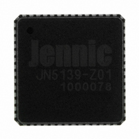
JN5139-Z01-V NXP Semiconductors, JN5139-Z01-V Datasheet - Page 81

JN5139-Z01-V
Manufacturer Part Number
JN5139-Z01-V
Description
IC MCU ZIGBEE 32BIT 2.4G 56QFN
Manufacturer
NXP Semiconductors
Series
JN5139-Z01Rxr
Specifications of JN5139-Z01-V
Frequency
2.4GHz
Modulation Or Protocol
802.15.4 Zigbee
Applications
General Purpose
Power - Output
3dBm
Sensitivity
-97dBm
Voltage - Supply
2.2 V ~ 3.6 V
Current - Receiving
34mA
Current - Transmitting
34mA
Data Interface
PCB, Surface Mount
Memory Size
96kB RAM, 192kB ROM
Antenna Connector
PCB, Surface Mount
Operating Temperature
-40°C ~ 85°C
Package / Case
56-QFN
Lead Free Status / RoHS Status
Lead free / RoHS Compliant
Data Rate - Maximum
-
Other names
616-1034-2
935293943515
JN5139-Z01-AI
JN5139-Z01-V
JN5139-Z01R1-ARV
JN5139-Z01R1V
935293943515
JN5139-Z01-AI
JN5139-Z01-V
JN5139-Z01R1-ARV
JN5139-Z01R1V
Disclaimers
The contents of this document are subject to change without notice. Jennic reserves the right to make changes,
without notice, in the products, including circuits and/or software, described or contained herein. Information
contained in this document regarding device applications and the like is intended through suggestion only and may
be superseded by updates. It is your responsibility to ensure that your application meets with your specifications.
Jennic warrants performance of its hardware products to the specifications applicable at the time of sale in
accordance with Jennic’s standard warranty. Testing and other quality control techniques are used to the extent
Jennic deems necessary to support this warranty. Except where mandatory by government requirements, testing of
all parameters of each product is not necessarily performed.
Jennic assumes no responsibility or liability for the use of any of these products, conveys no license or title under any
patent, copyright, or mask work right to these products, and makes no representations or warranties that these
products are free from patent, copyright, or mask work infringement, unless otherwise specified.
Jennic products are not intended for use in life support systems, appliances or systems where malfunction of these
products can reasonably be expected to result in personal injury, death or severe property or environmental damage.
Jennic customers using or selling these products for use in such applications do so at their own risk and agree to fully
indemnify Jennic for any damages resulting from such use.
All products are sold subject to Jennic's terms and conditions of sale supplied at the time of order acknowledgment.
All trademarks are the property of their respective owners.
Version Control
© NXP Laboratories UK 2010
Version
1.0
1.1
1.2
1.3
1.4
1.5
1.6
1.7
1.8
1.9
Notes
22
9th February 2007 – Added solder reflow profile
16th July 2007 – uplifted to Preliminary status, typical specification updates, internal reset modifications
31st July 2007 – updates to DC current consumptions
26th October 2007 – updated applications information, added PCB decal including paddle details
23rd April 2008 – Internal only
26th September 2008 – added min/max specifications, incorporated known errata
3rd April 2009 – Datasheet fully revised
15th May 2009 – Tape and reel information revised
23rd November 2010 – References to NXP added and ordering information changed
rd
December 2006 - First Release
JN-DS-JN5139 1v9
81


