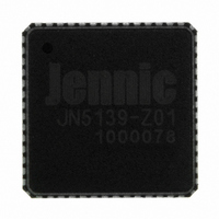
JN5139-Z01-V NXP Semiconductors, JN5139-Z01-V Datasheet - Page 44

JN5139-Z01-V
Manufacturer Part Number
JN5139-Z01-V
Description
IC MCU ZIGBEE 32BIT 2.4G 56QFN
Manufacturer
NXP Semiconductors
Series
JN5139-Z01Rxr
Specifications of JN5139-Z01-V
Frequency
2.4GHz
Modulation Or Protocol
802.15.4 Zigbee
Applications
General Purpose
Power - Output
3dBm
Sensitivity
-97dBm
Voltage - Supply
2.2 V ~ 3.6 V
Current - Receiving
34mA
Current - Transmitting
34mA
Data Interface
PCB, Surface Mount
Memory Size
96kB RAM, 192kB ROM
Antenna Connector
PCB, Surface Mount
Operating Temperature
-40°C ~ 85°C
Package / Case
56-QFN
Lead Free Status / RoHS Status
Lead free / RoHS Compliant
Data Rate - Maximum
-
Other names
616-1034-2
935293943515
JN5139-Z01-AI
JN5139-Z01-V
JN5139-Z01R1-ARV
JN5139-Z01R1V
935293943515
JN5139-Z01-AI
JN5139-Z01-V
JN5139-Z01R1-ARV
JN5139-Z01R1V
14 Two-Wire Serial interface
The JN5139 includes an industry standard two-wire synchronous serial interface (SIF) that provides a simple and
efficient method of data exchange between devices. The system operates as a master only and uses a serial data
line (SIF_D) and a serial clock line (SIF_CLK) to perform bi-directional data transfers; includes the following features:
The software libraries allow full control of the underlying registers and give access to the following features.
A configurable prescale register allows the interface to be configured to operate at up to 400kbit/s. The clock
generator handles the clock stretching required by some slave devices.
The Byte Command Controller handles traffic at the byte level. It takes data from the Command Register and
translates it into sequences based on the transmission of a single byte. By setting the start, stop, read, write and
acknowledge control bits in the command register it is possible to generate read or write sequences on the bus.
The data I/O shift register contains the data associated with the current transfer. During a read operation, data is
shifted into this register from the SIF_D line. When the read is complete the byte is copied into the receive register
and can be accessed.
During a write operation the contents of the transmit register are copied into the shift register and then onto the SIF_D
line. It is possible to generate an interrupt upon the completion of a byte transmission or reception. If interrupt-driven
communication is not desired it is possible to poll the status of the interface.
44
•
•
•
•
•
•
•
Compatible with both I
Software programmable clock frequency
Clock stretching and wait state generation
Software programmable acknowledge bit
Interrupt or bit-polling driven byte-by-byte data-transfers
Bus busy detection
Support for 7 and 10 bit addressing modes
Command
Prescale
Transmit
Register
Register
Register
Register
Register
Receive
Status
2
C and SMbus peripherals (master only mode)
Figure 35: SIF Block Diagram
JN-DS-JN5139 1v9
Command
Controller
Data I/O
Register
Byte
Shift
Command
Generator
Controller
Clock
Bit
© NXP Laboratories UK 2010
SIF_CLK
SIF_D


