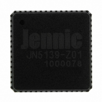
JN5139-Z01-V NXP Semiconductors, JN5139-Z01-V Datasheet - Page 23

JN5139-Z01-V
Manufacturer Part Number
JN5139-Z01-V
Description
IC MCU ZIGBEE 32BIT 2.4G 56QFN
Manufacturer
NXP Semiconductors
Series
JN5139-Z01Rxr
Specifications of JN5139-Z01-V
Frequency
2.4GHz
Modulation Or Protocol
802.15.4 Zigbee
Applications
General Purpose
Power - Output
3dBm
Sensitivity
-97dBm
Voltage - Supply
2.2 V ~ 3.6 V
Current - Receiving
34mA
Current - Transmitting
34mA
Data Interface
PCB, Surface Mount
Memory Size
96kB RAM, 192kB ROM
Antenna Connector
PCB, Surface Mount
Operating Temperature
-40°C ~ 85°C
Package / Case
56-QFN
Lead Free Status / RoHS Status
Lead free / RoHS Compliant
Data Rate - Maximum
-
Other names
616-1034-2
935293943515
JN5139-Z01-AI
JN5139-Z01-V
JN5139-Z01R1-ARV
JN5139-Z01R1V
935293943515
JN5139-Z01-AI
JN5139-Z01-V
JN5139-Z01R1-ARV
JN5139-Z01R1V
8 Wireless Transceiver
The wireless transceiver comprises a 2.45GHz radio, an O-QPSK modem, a baseband processor, a security
coprocessor and PHY controller. These blocks, with protocol software provided as a library, implement an
IEEE802.15.4 standards-based wireless transceiver that transmits and receives data over the air in the unlicensed
2.4GHz band.
8.1 Radio
The radio comprises a low-IF receive path and a direct up-conversion transmit path, which converge at the TX/RX
switch. This switch includes the necessary matching components such that a 200Ω differential antenna may be
directly connected without external components. Alternatively, a balun can be used for single ended antennas.
The 16MHz crystal oscillator feeds a divider, which provides the frequency synthesiser with a reference
frequency. The synthesiser contains programmable feedback dividers, phase detector, charge pump and internal
Voltage Controlled Oscillator (VCO). The VCO has no external components, and includes calibration circuitry to
compensate for differences in internal component values due to process and temperature variations. The VCO is
controlled by a Phase Locked Loop (PLL) that has a loop filter comprising 3 external components. A programmable
charge pump is also used to tune the loop characteristic. Finally, quadrature (I and Q) local oscillator signals for the
mixer drives are derived.
The receiver chain starts with the low noise amplifier / mixer combination whose outputs are passed to the polyphase
bandpass filter. This filter provides the channel definition as well as image frequency rejection. The signal is then
passed to two variable gain amplifier blocks. The gain control for these stages and the bandpass filter is derived in
the automatic gain control (AGC) block within the Modem. The signal is conditioned with the anti-alias low pass filter
before being converted to a digital signal with a flash ADC.
In the transmit direction, the digital I and Q streams from the Modem are passed to I and Q quadrature DAC blocks
which are buffered and low-pass filtered, before being applied to the modulator mixers. The summed 2.4 GHz signal
is then passed to the RF Power Amplifier (PA), whose power control can be selected from one of six settings. The
output of the PA drives the antenna via the RX/TX switch.
© NXP Laboratories UK 2010
RX
TX
LOQ
LOI
LNA
Power
PA
PA
90
0
∑
LOQ
LOI
PLL
Figure 14: Radio Architecture
LOQ
LOI
JN-DS-JN5139 1v9
Calibration
VCO
VGA1
VGA2
Calibration
PA (Q)
PA (I)
Trim
Trim
VGA
VGA
Reference
& BIAS
DAC
DAC
ADC
IF DATA
QDATA
IDATA
AGC
23


