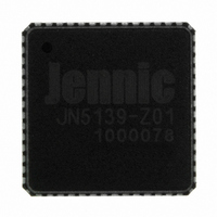
JN5139-Z01-V NXP Semiconductors, JN5139-Z01-V Datasheet - Page 61

JN5139-Z01-V
Manufacturer Part Number
JN5139-Z01-V
Description
IC MCU ZIGBEE 32BIT 2.4G 56QFN
Manufacturer
NXP Semiconductors
Series
JN5139-Z01Rxr
Specifications of JN5139-Z01-V
Frequency
2.4GHz
Modulation Or Protocol
802.15.4 Zigbee
Applications
General Purpose
Power - Output
3dBm
Sensitivity
-97dBm
Voltage - Supply
2.2 V ~ 3.6 V
Current - Receiving
34mA
Current - Transmitting
34mA
Data Interface
PCB, Surface Mount
Memory Size
96kB RAM, 192kB ROM
Antenna Connector
PCB, Surface Mount
Operating Temperature
-40°C ~ 85°C
Package / Case
56-QFN
Lead Free Status / RoHS Status
Lead free / RoHS Compliant
Data Rate - Maximum
-
Other names
616-1034-2
935293943515
JN5139-Z01-AI
JN5139-Z01-V
JN5139-Z01R1-ARV
JN5139-Z01R1V
935293943515
JN5139-Z01-AI
JN5139-Z01-V
JN5139-Z01R1-ARV
JN5139-Z01R1V
17.3.11
VDD = 2.2 to 3.6V -40 to +85ºC
17.3.12
17.3.13
The JN5139 meets all the requirements of the IEEE802.15.4 standard for 2.2-3.6V and offers the following improved
RF characteristics. All RF characteristics are measured single ended and include the losses of a ceramic balun.
This part also meets the following regulatory body approvals, when used with Jennic’s Module Reference Designs.
Compliant with FCC part 15, rules, IC Canada, ETSI ETS 300-328 and Japan ARIB STD-T66
© NXP Laboratories UK 2010
Type
Impedance
Frequency range
Analogue response time
(normal)
Total response time
(normal) including delay to
Interrupt controller
Analogue response time
(low power)
Hysteresis
Vref (Internal)
Common Mode input range
Current (normal mode)
Current (low power mode)
Operating Range
Sensor Gain
Accuracy
Non-linearity
Output Voltage
Typical Voltage
Resolution
Parameter
Parameter
Parameter
Comparators
Temperature Sensor
Radio Transceiver
0.154
-1.44
Min
630
-40
See Section 17.3.8 Bandgap Reference
-
-
Min
12
28
40
2.400 GHz
4
0
Min
0.182
RF Port Characteristics
-1.55
Typ
745
745
-
-
-
JN-DS-JN5139 1v9
67.5
Typ
105
2.4
1.2
10
20
40
200ohm
Typical
0.209
-1.66
Max
±10
855
2.5
85
105 + 125
Max
Vdd
140
16
26
50
90
°C/LSB
mV/°C
Unit
mV
mV
°C
°C
°C
2.485GHz
Max
Unit
mV
µA
µA
ns
ns
µs
V
V
Includes absolute variation
due to manufacturing & temp
Typical at 3.0V 25°C
0 to Vref ADC I/P Range
Differential
2.4-2.5GHz
+/- 250mV overdrive
10pF load
Digital delay can be
up to a max. of two
16MHz clock periods
+/- 250mV overdrive
No digital delay
Programmable in 3
steps and zero.
Notes
Notes
Notes
61


