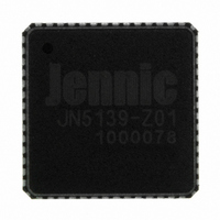
JN5139-Z01-V NXP Semiconductors, JN5139-Z01-V Datasheet - Page 45

JN5139-Z01-V
Manufacturer Part Number
JN5139-Z01-V
Description
IC MCU ZIGBEE 32BIT 2.4G 56QFN
Manufacturer
NXP Semiconductors
Series
JN5139-Z01Rxr
Specifications of JN5139-Z01-V
Frequency
2.4GHz
Modulation Or Protocol
802.15.4 Zigbee
Applications
General Purpose
Power - Output
3dBm
Sensitivity
-97dBm
Voltage - Supply
2.2 V ~ 3.6 V
Current - Receiving
34mA
Current - Transmitting
34mA
Data Interface
PCB, Surface Mount
Memory Size
96kB RAM, 192kB ROM
Antenna Connector
PCB, Surface Mount
Operating Temperature
-40°C ~ 85°C
Package / Case
56-QFN
Lead Free Status / RoHS Status
Lead free / RoHS Compliant
Data Rate - Maximum
-
Other names
616-1034-2
935293943515
JN5139-Z01-AI
JN5139-Z01-V
JN5139-Z01R1-ARV
JN5139-Z01R1V
935293943515
JN5139-Z01-AI
JN5139-Z01-V
JN5139-Z01R1-ARV
JN5139-Z01R1V
The first byte of data transferred by the device after a start bit is the slave address. The JN5139 supports both 7-bit
and 10-bit slave addresses by generating either one or two address transfers. Only the slave with a matching
address will respond by returning an acknowledge bit.
14.1 Connecting Devices
The clock and data lines, SIF_D and SIF_CLK, are alternative functions of DIO lines 15 and 14 respectively. The
serial interface function of these pins is selected when the interface is enabled. They are both bi-directional lines,
connected internally to the positive supply voltage via weak (45kΩ) programmable pull-up resistors. However, it is
recommended that external 4.7kΩ pull-ups be used for reliable operation at high bus speeds, as shown in Figure 36.
When the bus is free, both lines are HIGH. The output stages of devices connected to the bus must have an open-
drain or open-collector in order to perform the wired-AND function. The number of devices connected to the bus is
solely dependent on the bus capacitance limit of 400pF.
14.2 Clock Stretching
Slave devices can use clock stretching to slow down the transfer bit rate. After the master has driven SIF_CLK low,
the slave can drive SIF_CLK low for the required period and then release it. If the slave’s SIF_CLK low period is
greater than the master’s low period, the resulting SIF_CLK bus signal low period is stretched thus inserting wait
states.
© NXP Laboratories UK 2010
JN5139
SIF
SIF_CLK
SIF_CLK
SIF_CLK
55
56
SIF_CLK
SIF_D
D1_OUT
D1_IN
Figure 36 Connection Details
Figure 37 Clock Stretching
DEVICE 1
CLK1_OUT
CLK1_IN
JN-DS-JN5139 1v9
Clock held low
by Slave
R
P
R
D2_IN
D2_OUT
P
Master SIF_CLK
Slave SIF_CLK
Wired-AND SIF_CLK
Pullup
Resistors
Vdd
DEVICE 2
CLK2_OUT
CLK2_IN
45


