AMIS-52150-XTD ON Semiconductor, AMIS-52150-XTD Datasheet - Page 10
AMIS-52150-XTD
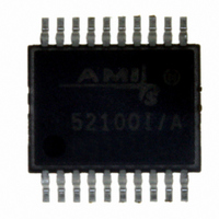
Manufacturer Part Number
AMIS-52150-XTD
Description
TXRX RF SUB 1GHZ CDR 20-SSOP
Manufacturer
ON Semiconductor
Datasheet
1.AMIS-52150-XTD.pdf
(25 pages)
Specifications of AMIS-52150-XTD
Frequency
300Mhz ~ 768MHz
Data Rate - Maximum
16kbps
Modulation Or Protocol
ASK, OOK
Applications
Wireless Modules
Power - Output
12dBm
Sensitivity
-117dBm
Voltage - Supply
2.3 V ~ 3.6 V
Current - Receiving
7.5mA
Current - Transmitting
25mA
Data Interface
PCB, Surface Mount
Antenna Connector
PCB, Surface Mount
Operating Temperature
0°C ~ 50°C
Package / Case
20-SSOP
Ic Interface Type
I2C
No. Of Tx Buffers
1
No. Of Rx Buffers
1
No. Of Filters
1
No. Of Interrupts
1
Supply Voltage Range
2.3V To 3.6V
Digital Ic Case Style
SSOP
No. Of Pins
20
Rohs Compliant
No
Operating Temperature (min)
0C
Operating Temperature Classification
Commercial
Modulation Type
ASK/OOK
Operating Supply Voltage (min)
2.3V
Operating Supply Voltage (typ)
3V
Operating Supply Voltage (max)
3.6V
Lead Free Status / RoHS Status
Lead free / RoHS Compliant
Memory Size
-
Lead Free Status / Rohs Status
Not Compliant
Other names
766-1020
Available stocks
Company
Part Number
Manufacturer
Quantity
Price
Company:

Part Number:
AMIS-52150-XTD
Manufacturer:
ON Semiconductor
Quantity:
135


AMIS-52150
Table 16: I
Table 17: I
The I
is activated upon detection of RF energy during Sniff Mode
device in order to alert an external controller to perform specific tasks, as defined by the system designer.
8.10 TX/RX, Data Input/Output Pin
The transmit/receive (TX/RX) pin can be programmed to be either an input for RF transmissions, or an output for RF reception, or the
output of the RC oscillator signal, or the output of the recovered data from the CDR circuits, respectively.
In transmit mode, this pin is the digital data input to the AMIS-52150 RF transmit circuit. The digital data results in the On and Off
cycling of the output power amplifier (PA). The AMIS-52150 does not perform any protocol conversion on the data bit stream; it is
simply a serial bit stream. The state of the TX/RX pin either turns the output amplifier On (enabling RF transmission) or turns the output
amplifier Off (disabling RF transmission). The TX/RX input can be inverted which causes the state control of the RF output amplifier to
be inverted as well.
In receive mode, this pin is the digital data output from the AMIS-52150 receivers. The received data is recovered as a high/low (digital
ones and zeros) serial bit stream; the AMIS-52150 does not modify the received data protocol. The data output state due to the
presence of energy in the receiver can be programmed to be either a high level or a low level at the TX/RX pin. An external controller is
needed to decode the information in the recovered data bit stream.
When programmed to be an oscillator output, the TX/RX pin outputs the signal from the RC oscillator. This signal can be used to
monitor the frequency of the RC oscillator in order to trim the frequency to the desired value.
The TX/RX pin can be programmed to output the recovered data obtained from the clock and data recovery circuits. In this case, the
device must be programmed in the CDR mode. More information on CDR will be provided in a later section of this datasheet.
The functions of the TX/RX port are controlled by the values of the register settings, as shown in Table 18.
Table 18: TX/RX Pin Definition Control Registers
8.11 VDD, Supply Voltage Pin
The VDD pin is the power supply pin for the AMIS-52150. The voltage on this pin is typically 3.0V. Please refer to the section
“Operating and Maximum Specifications” of this document for the VDD operating conditions.
I
Register (HEX)
Register (HEX)
2
I
AMIS-52150
AMIS-52150
C Control Register
2
I
2
CDATA
CCLK
Pin
Device
2
CDATA and I
0x0c
0x0e
0x1e
2
2
C Bus Device Addressing
C Control Register
Function
Internal pull-up R
Internal pull-up R
Address (Bin)
01101000
01101001
2
Name
I
increment
Name
RC OSC on TX/RX
TX/RX invert
2
CCLK lines are also used to signal to an external controller certain internal activities of the transceiver. The receiver
C address
HEX
Bits
68
69
2
Typ.
15
15
Function
Device write
Device read
Bits
States
2
5
0
1
Units
KΩ
KΩ
Rev. 7 | Page 10 of 25 | www.onsemi.com
States
Comments
Increment after write
Do not increment
0
1
0
1
Comments
RX/TX normal
RC OSC output
Normal levels
Inverted
TM
operation. The wake-up timer can also be configured to wake-up the
Related parts for AMIS-52150-XTD
Image
Part Number
Description
Manufacturer
Datasheet
Request
R

Part Number:
Description:
ON Semiconductor [VOLTAGE REGULATOR]
Manufacturer:
ON Semiconductor
Datasheet:
Part Number:
Description:
357-036-542-201 CARDEDGE 36POS DL .156 BLK LOPRO
Manufacturer:
ON Semiconductor
Datasheet:
Part Number:
Description:
357-036-542-201 CARDEDGE 36POS DL .156 BLK LOPRO
Manufacturer:
ON Semiconductor
Datasheet:
Part Number:
Description:
357-036-542-201 CARDEDGE 36POS DL .156 BLK LOPRO
Manufacturer:
ON Semiconductor
Datasheet:
Part Number:
Description:
357-036-542-201 CARDEDGE 36POS DL .156 BLK LOPRO
Manufacturer:
ON Semiconductor
Datasheet:
Part Number:
Description:
357-036-542-201 CARDEDGE 36POS DL .156 BLK LOPRO
Manufacturer:
ON Semiconductor
Datasheet:
Part Number:
Description:
357-036-542-201 CARDEDGE 36POS DL .156 BLK LOPRO
Manufacturer:
ON Semiconductor
Datasheet:
Part Number:
Description:
357-036-542-201 CARDEDGE 36POS DL .156 BLK LOPRO
Manufacturer:
ON Semiconductor
Datasheet:
Part Number:
Description:
357-036-542-201 CARDEDGE 36POS DL .156 BLK LOPRO
Manufacturer:
ON Semiconductor
Datasheet:
Part Number:
Description:
357-036-542-201 CARDEDGE 36POS DL .156 BLK LOPRO
Manufacturer:
ON Semiconductor
Datasheet:
Part Number:
Description:
357-036-542-201 CARDEDGE 36POS DL .156 BLK LOPRO
Manufacturer:
ON Semiconductor
Datasheet:
Part Number:
Description:
Manufacturer:
ON Semiconductor
Datasheet:
Part Number:
Description:
Manufacturer:
ON Semiconductor
Datasheet:
Part Number:
Description:
Manufacturer:
ON Semiconductor
Datasheet: