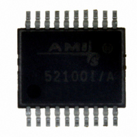
AMIS-52150-XTD ON Semiconductor, AMIS-52150-XTD Datasheet - Page 21

AMIS-52150-XTD
Manufacturer Part Number
AMIS-52150-XTD
Description
TXRX RF SUB 1GHZ CDR 20-SSOP
Manufacturer
ON Semiconductor
Datasheet
1.AMIS-52150-XTD.pdf
(25 pages)
Specifications of AMIS-52150-XTD
Frequency
300Mhz ~ 768MHz
Data Rate - Maximum
16kbps
Modulation Or Protocol
ASK, OOK
Applications
Wireless Modules
Power - Output
12dBm
Sensitivity
-117dBm
Voltage - Supply
2.3 V ~ 3.6 V
Current - Receiving
7.5mA
Current - Transmitting
25mA
Data Interface
PCB, Surface Mount
Antenna Connector
PCB, Surface Mount
Operating Temperature
0°C ~ 50°C
Package / Case
20-SSOP
Ic Interface Type
I2C
No. Of Tx Buffers
1
No. Of Rx Buffers
1
No. Of Filters
1
No. Of Interrupts
1
Supply Voltage Range
2.3V To 3.6V
Digital Ic Case Style
SSOP
No. Of Pins
20
Rohs Compliant
No
Operating Temperature (min)
0C
Operating Temperature Classification
Commercial
Modulation Type
ASK/OOK
Operating Supply Voltage (min)
2.3V
Operating Supply Voltage (typ)
3V
Operating Supply Voltage (max)
3.6V
Lead Free Status / RoHS Status
Lead free / RoHS Compliant
Memory Size
-
Lead Free Status / Rohs Status
Not Compliant
Other names
766-1020
Available stocks
Company
Part Number
Manufacturer
Quantity
Price
Company:
Part Number:
AMIS-52150-XTD
Manufacturer:
ON Semiconductor
Quantity:
135
AMIS-52150
recovery (see the application note titled “AMIS-52150 Clock and Data Recovery Circuit Operation and Set-Up”), the register shown in
Table 28 can be used to define the test mode operation.
Table 28: Clock and Data Recovery Test Mode
9.7 Wake-Up Function
Ultra-low power applications can take advantage of the wake-up function of the AMIS-52150. The AMIS-52150 can be placed in a low
power or “sleep” state until an interrupt based on the programmable wake-up timer is generated. This wakes up the transceiver, which
then flags the external microcontroller to perform the required application-specific operations. The wake-up interrupt is also generated
based on detection of RF energy (Sniff Mode
the AMIS-52150 is in the “sleep’” state, the wake-up signal can be generated by the microcontroller. Table 29 lists the registers
associated with the wake-up function.
Table 29: Application Wake-Up Control Registers
9.8 I
The I
data pin is clocked into or out of the AMIS-52150 by the clock pin. The AMIS-52150 is implemented as a slave device, which means
that the external controller is the master device. The clock signal for all transmissions between the master (controller) and the slave
(AMIS-52150) is generated by the controller. The serial communication bit rate can be as high as 400Kbps. A communication link is
initiated based on a start sequence. Bi-directional communication continues as long as the master and slave acknowledge the write or
read sequences, and is terminated with a stop sequence. This is illustrated in Figure 15, Figure 16 and Figure 17, respectively.
Clock and Data Recovery Test Control Register
Register (HEX)
Application Wakeup Control Registers
Register (HEX)
2
C Interface
2
C is a two pin bi-directional serial interface communication bus, with a data line and a clock line, respectively. Serial data on the
0x1d
0x14
0x15
0x17
Binary Code
00001110
00001111
Name
AW TIMER DIV
AW TIMER
PRE/POST AW
DELAY
HEX Code
0x0e
0x0f
Bits
All
All
All
TM
). Communication with the microcontroller takes place via the I
States
Rev. 7 | Page 21 of 25 | www.onsemi.com
Comments
Normal RSSI digital input
CDR start bit digital input to RSSI
Comments
Divides the RC oscillator to form a clock for the AW
Number of AW clock periods before a AW wakeup
Number of CLKOUT clock periods before the TX/RX pin
goes low for a AW cycle
2
C bus. In addition, when


