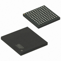
ATMEGA2560R231-AU Atmel, ATMEGA2560R231-AU Datasheet - Page 147

ATMEGA2560R231-AU
Manufacturer Part Number
ATMEGA2560R231-AU
Description
BUNDLE ATMEGA2560/RF231 TQFP
Manufacturer
Atmel
Datasheet
1.ATMEGA640V-8CU.pdf
(444 pages)
Specifications of ATMEGA2560R231-AU
Frequency
2.4GHz
Modulation Or Protocol
802.15.4 Zigbee, 6LoWPAN, RF4CE, SP100, WirelessHART™, ISM
Data Interface
PCB, Surface Mount
Memory Size
256kB Flash, 4kB EEPROM, 8kB RAM
Antenna Connector
PCB, Surface Mount
Package / Case
100-TFBGA
Processor Series
ATMEGA256x
Core
AVR8
Data Bus Width
8 bit
Program Memory Type
Flash
Program Memory Size
256 KB
Data Ram Size
8 KB
Development Tools By Supplier
ATAVRRZ541, ATAVRRAVEN, ATAVRRZRAVEN
Lead Free Status / RoHS Status
Lead free / RoHS Compliant
Voltage - Supply
-
Power - Output
-
Operating Temperature
-
Applications
-
Sensitivity
-
Data Rate - Maximum
-
Current - Transmitting
-
Current - Receiving
-
Lead Free Status / Rohs Status
Details
- Current page: 147 of 444
- Download datasheet (10Mb)
16.8
16.8.1
2549M–AVR–09/10
Compare Match Output Unit
Compare Output Mode and Waveform Generation
The Compare Output mode (COMnx1:0) bits have two functions. The Waveform Generator uses
the COMnx1:0 bits for defining the Output Compare (OCnx) state at the next compare match.
Secondly the COMnx1:0 bits control the OCnx pin output source.
schematic of the logic affected by the COMnx1:0 bit setting. The I/O Registers, I/O bits, and I/O
pins in the figure are shown in bold. Only the parts of the general I/O Port Control Registers
(DDR and PORT) that are affected by the COMnx1:0 bits are shown. When referring to the
OCnx state, the reference is for the internal OCnx Register, not the OCnx pin. If a system reset
occur, the OCnx Register is reset to “0”.
Figure 16-5. Compare Match Output Unit, Schematic
The general I/O port function is overridden by the Output Compare (OCnx) from the Waveform
Generator if either of the COMnx1:0 bits are set. However, the OCnx pin direction (input or out-
put) is still controlled by the Data Direction Register (DDR) for the port pin. The Data Direction
Register bit for the OCnx pin (DDR_OCnx) must be set as output before the OCnx value is visi-
ble on the pin. The port override function is generally independent of the Waveform Generation
mode, but there are some exceptions. Refer to
and
The design of the Output Compare pin logic allows initialization of the OCnx state before the out-
put is enabled. Note that some COMnx1:0 bit settings are reserved for certain modes of
operation.
The COMnx1:0 bits have no effect on the Input Capture unit.
The Waveform Generator uses the COMnx1:0 bits differently in normal, CTC, and PWM modes.
For all modes, setting the COMnx1:0 = 0 tells the Waveform Generator that no action on the
OCnx Register is to be performed on the next compare match. For compare output actions in the
Table 16-5 on page 160
COMnx1
COMnx0
FOCnx
clk
I/O
See “Register Description” on page 158.
Waveform
Generator
for details.
ATmega640/1280/1281/2560/2561
D
D
D
PORT
DDR
OCnx
Table 16-3 on page
Q
Q
Q
1
0
Figure 16-5
159,
Table 16-4 on page 159
shows a simplified
OCnx
Pin
147
Related parts for ATMEGA2560R231-AU
Image
Part Number
Description
Manufacturer
Datasheet
Request
R

Part Number:
Description:
Manufacturer:
ATMEL Corporation
Datasheet:

Part Number:
Description:
IC AVR MCU 256K 16MHZ 100TQFP
Manufacturer:
Atmel
Datasheet:

Part Number:
Description:
MCU AVR 256K FLASH 16MHZ 100TQFP
Manufacturer:
Atmel
Datasheet:

Part Number:
Description:
MCU AVR 256K FLASH 16MHZ 100CBGA
Manufacturer:
Atmel
Datasheet:

Part Number:
Description:
IC MCU AVR 256K FLASH 100-CBGA
Manufacturer:
Atmel
Datasheet:

Part Number:
Description:
IC AVR MCU 256K 16MHZ 100TQFP
Manufacturer:
Atmel
Datasheet:

Part Number:
Description:
DEV KIT FOR AVR/AVR32
Manufacturer:
Atmel
Datasheet:

Part Number:
Description:
INTERVAL AND WIPE/WASH WIPER CONTROL IC WITH DELAY
Manufacturer:
ATMEL Corporation
Datasheet:

Part Number:
Description:
Low-Voltage Voice-Switched IC for Hands-Free Operation
Manufacturer:
ATMEL Corporation
Datasheet:

Part Number:
Description:
MONOLITHIC INTEGRATED FEATUREPHONE CIRCUIT
Manufacturer:
ATMEL Corporation
Datasheet:


