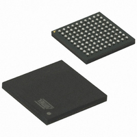
ATMEGA2560R231-AU Atmel, ATMEGA2560R231-AU Datasheet - Page 91

ATMEGA2560R231-AU
Manufacturer Part Number
ATMEGA2560R231-AU
Description
BUNDLE ATMEGA2560/RF231 TQFP
Manufacturer
Atmel
Datasheet
1.ATMEGA640V-8CU.pdf
(444 pages)
Specifications of ATMEGA2560R231-AU
Frequency
2.4GHz
Modulation Or Protocol
802.15.4 Zigbee, 6LoWPAN, RF4CE, SP100, WirelessHART™, ISM
Data Interface
PCB, Surface Mount
Memory Size
256kB Flash, 4kB EEPROM, 8kB RAM
Antenna Connector
PCB, Surface Mount
Package / Case
100-TFBGA
Processor Series
ATMEGA256x
Core
AVR8
Data Bus Width
8 bit
Program Memory Type
Flash
Program Memory Size
256 KB
Data Ram Size
8 KB
Development Tools By Supplier
ATAVRRZ541, ATAVRRAVEN, ATAVRRZRAVEN
Lead Free Status / RoHS Status
Lead free / RoHS Compliant
Voltage - Supply
-
Power - Output
-
Operating Temperature
-
Applications
-
Sensitivity
-
Data Rate - Maximum
-
Current - Transmitting
-
Current - Receiving
-
Lead Free Status / Rohs Status
Details
- Current page: 91 of 444
- Download datasheet (10Mb)
2549M–AVR–09/10
• OC0B – Port G, Bit 5
OC0B, Output Compare match B output: The PG5 pin can serve as an external output for the
TImer/Counter0 Output Compare. The pin has to be configured as an output (DDG5 set) to
serve this function. The OC0B pin is also the output pin for the PWM mode timer function.
• TOSC1 – Port G, Bit 4
TOSC2, Timer Oscillator pin 1: When the AS2 bit in ASSR is set (one) to enable asynchronous
clocking of Timer/Counter2, pin PG4 is disconnected from the port, and becomes the input of the
inverting Oscillator amplifier. In this mode, a Crystal Oscillator is connected to this pin, and the
pin can not be used as an I/O pin.
• TOSC2 – Port G, Bit 3
TOSC2, Timer Oscillator pin 2: When the AS2 bit in ASSR is set (one) to enable asynchronous
clocking of Timer/Counter2, pin PG3 is disconnected from the port, and becomes the inverting
output of the Oscillator amplifier. In this mode, a Crystal Oscillator is connected to this pin, and
the pin can not be used as an I/O pin.
• ALE – Port G, Bit 2
ALE is the external data memory Address Latch Enable signal.
• RD – Port G, Bit 1
RD is the external data memory read control strobe.
• WR – Port G, Bit 0
WR is the external data memory write control strobe.
Table 12-22 on page 91
the overriding signals shown in
Table 12-22. Overriding Signals for Alternate Functions in PG5:PG4
Signal Name
DIEOE
DIEOV
PUOE
DDOE
DDOV
PUOV
PVOE
PVOV
PTOE
AIO
DI
and
—
–
–
–
–
–
–
–
–
–
–
–
Table 12-23 on page 92
Figure 12-5 on page
ATmega640/1280/1281/2560/2561
—
–
–
–
–
–
–
–
–
–
–
–
76.
relates the alternate functions of Port G to
OC0B Enable
PG5/OC0B
OC0B
–
–
–
–
–
–
–
–
–
T/C2 OSC INPUT
PG4/TOSC1
EXCLK
AS2
AS2
AS2
0
0
0
0
–
–
91
Related parts for ATMEGA2560R231-AU
Image
Part Number
Description
Manufacturer
Datasheet
Request
R

Part Number:
Description:
Manufacturer:
ATMEL Corporation
Datasheet:

Part Number:
Description:
IC AVR MCU 256K 16MHZ 100TQFP
Manufacturer:
Atmel
Datasheet:

Part Number:
Description:
MCU AVR 256K FLASH 16MHZ 100TQFP
Manufacturer:
Atmel
Datasheet:

Part Number:
Description:
MCU AVR 256K FLASH 16MHZ 100CBGA
Manufacturer:
Atmel
Datasheet:

Part Number:
Description:
IC MCU AVR 256K FLASH 100-CBGA
Manufacturer:
Atmel
Datasheet:

Part Number:
Description:
IC AVR MCU 256K 16MHZ 100TQFP
Manufacturer:
Atmel
Datasheet:

Part Number:
Description:
DEV KIT FOR AVR/AVR32
Manufacturer:
Atmel
Datasheet:

Part Number:
Description:
INTERVAL AND WIPE/WASH WIPER CONTROL IC WITH DELAY
Manufacturer:
ATMEL Corporation
Datasheet:

Part Number:
Description:
Low-Voltage Voice-Switched IC for Hands-Free Operation
Manufacturer:
ATMEL Corporation
Datasheet:

Part Number:
Description:
MONOLITHIC INTEGRATED FEATUREPHONE CIRCUIT
Manufacturer:
ATMEL Corporation
Datasheet:


