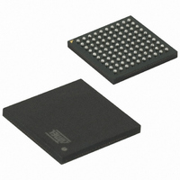
ATMEGA2560R231-AU Atmel, ATMEGA2560R231-AU Datasheet - Page 161

ATMEGA2560R231-AU
Manufacturer Part Number
ATMEGA2560R231-AU
Description
BUNDLE ATMEGA2560/RF231 TQFP
Manufacturer
Atmel
Datasheet
1.ATMEGA640V-8CU.pdf
(444 pages)
Specifications of ATMEGA2560R231-AU
Frequency
2.4GHz
Modulation Or Protocol
802.15.4 Zigbee, 6LoWPAN, RF4CE, SP100, WirelessHART™, ISM
Data Interface
PCB, Surface Mount
Memory Size
256kB Flash, 4kB EEPROM, 8kB RAM
Antenna Connector
PCB, Surface Mount
Package / Case
100-TFBGA
Processor Series
ATMEGA256x
Core
AVR8
Data Bus Width
8 bit
Program Memory Type
Flash
Program Memory Size
256 KB
Data Ram Size
8 KB
Development Tools By Supplier
ATAVRRZ541, ATAVRRAVEN, ATAVRRZRAVEN
Lead Free Status / RoHS Status
Lead free / RoHS Compliant
Voltage - Supply
-
Power - Output
-
Operating Temperature
-
Applications
-
Sensitivity
-
Data Rate - Maximum
-
Current - Transmitting
-
Current - Receiving
-
Lead Free Status / Rohs Status
Details
- Current page: 161 of 444
- Download datasheet (10Mb)
16.11.9
2549M–AVR–09/10
TCCR1C – Timer/Counter 1 Control Register C
• Bit 6 – ICESn: Input Capture Edge Select
This bit selects which edge on the Input Capture Pin (ICPn) that is used to trigger a capture
event. When the ICESn bit is written to zero, a falling (negative) edge is used as trigger, and
when the ICESn bit is written to one, a rising (positive) edge will trigger the capture.
When a capture is triggered according to the ICESn setting, the counter value is copied into the
Input Capture Register (ICRn). The event will also set the Input Capture Flag (ICFn), and this
can be used to cause an Input Capture Interrupt, if this interrupt is enabled.
When the ICRn is used as TOP value (see description of the WGMn3:0 bits located in the
TCCRnA and the TCCRnB Register), the ICPn is disconnected and consequently the input cap-
ture function is disabled.
• Bit 5 – Reserved Bit
This bit is reserved for future use. For ensuring compatibility with future devices, this bit must be
written to zero when TCCRnB is written.
• Bit 4:3 – WGMn3:2: Waveform Generation Mode
See TCCRnA Register description.
• Bit 2:0 – CSn2:0: Clock Select
The three clock select bits select the clock source to be used by the Timer/Counter, see
16-10 on page 156
Table 16-6.
If external pin modes are used for the Timer/Countern, transitions on the Tn pin will clock the
counter even if the pin is configured as an output. This feature allows software control of the
counting.
Bit
(0x82)
Read/Write
Initial Value
CSn2
0
0
0
0
1
1
1
1
CSn1
0
0
1
1
0
0
1
1
Clock Select Bit Description
FOC1A
W
7
0
and
CSn0
Figure 16-11 on page
FOC1B
0
1
0
1
0
1
0
1
W
6
0
ATmega640/1280/1281/2560/2561
FOC1C
W
5
0
External clock source on Tn pin. Clock on falling edge
External clock source on Tn pin. Clock on rising edge
No clock source. (Timer/Counter stopped)
R
4
–
0
156.
clk
clk
clk
clk
I/O
clk
R
I/O
3
–
0
I/O
I/O
/1024 (From prescaler)
/256 (From prescaler)
I/O
/64 (From prescaler)
/8 (From prescaler)
Description
/1 (No prescaling
R
2
–
0
R
1
0
–
R
0
–
0
TCCR1C
Figure
161
Related parts for ATMEGA2560R231-AU
Image
Part Number
Description
Manufacturer
Datasheet
Request
R

Part Number:
Description:
Manufacturer:
ATMEL Corporation
Datasheet:

Part Number:
Description:
IC AVR MCU 256K 16MHZ 100TQFP
Manufacturer:
Atmel
Datasheet:

Part Number:
Description:
MCU AVR 256K FLASH 16MHZ 100TQFP
Manufacturer:
Atmel
Datasheet:

Part Number:
Description:
MCU AVR 256K FLASH 16MHZ 100CBGA
Manufacturer:
Atmel
Datasheet:

Part Number:
Description:
IC MCU AVR 256K FLASH 100-CBGA
Manufacturer:
Atmel
Datasheet:

Part Number:
Description:
IC AVR MCU 256K 16MHZ 100TQFP
Manufacturer:
Atmel
Datasheet:

Part Number:
Description:
DEV KIT FOR AVR/AVR32
Manufacturer:
Atmel
Datasheet:

Part Number:
Description:
INTERVAL AND WIPE/WASH WIPER CONTROL IC WITH DELAY
Manufacturer:
ATMEL Corporation
Datasheet:

Part Number:
Description:
Low-Voltage Voice-Switched IC for Hands-Free Operation
Manufacturer:
ATMEL Corporation
Datasheet:

Part Number:
Description:
MONOLITHIC INTEGRATED FEATUREPHONE CIRCUIT
Manufacturer:
ATMEL Corporation
Datasheet:


