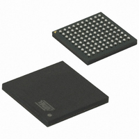
ATMEGA2560R231-AU Atmel, ATMEGA2560R231-AU Datasheet - Page 326

ATMEGA2560R231-AU
Manufacturer Part Number
ATMEGA2560R231-AU
Description
BUNDLE ATMEGA2560/RF231 TQFP
Manufacturer
Atmel
Datasheet
1.ATMEGA640V-8CU.pdf
(444 pages)
Specifications of ATMEGA2560R231-AU
Frequency
2.4GHz
Modulation Or Protocol
802.15.4 Zigbee, 6LoWPAN, RF4CE, SP100, WirelessHART™, ISM
Data Interface
PCB, Surface Mount
Memory Size
256kB Flash, 4kB EEPROM, 8kB RAM
Antenna Connector
PCB, Surface Mount
Package / Case
100-TFBGA
Processor Series
ATMEGA256x
Core
AVR8
Data Bus Width
8 bit
Program Memory Type
Flash
Program Memory Size
256 KB
Data Ram Size
8 KB
Development Tools By Supplier
ATAVRRZ541, ATAVRRAVEN, ATAVRRZRAVEN
Lead Free Status / RoHS Status
Lead free / RoHS Compliant
Voltage - Supply
-
Power - Output
-
Operating Temperature
-
Applications
-
Sensitivity
-
Data Rate - Maximum
-
Current - Transmitting
-
Current - Receiving
-
Lead Free Status / Rohs Status
Details
- Current page: 326 of 444
- Download datasheet (10Mb)
28.6.11
28.6.12
2549M–AVR–09/10
Preventing Flash Corruption
Programming Time for Flash when Using SPM
SPMCSR, the signature byte value will be loaded in the destination register. The SIGRD and
SPMEN bits will auto-clear upon completion of reading the Signature Row Lock bits or if no LPM
instruction is executed within three CPU cycles. When SIGRD and SPMEN are cleared, LPM will
work as described in the Instruction set Manual.
Table 28-5.
Note:
During periods of low V
too low for the CPU and the Flash to operate properly. These issues are the same as for board
level systems using the Flash, and the same design solutions should be applied.
A Flash program corruption can be caused by two situations when the voltage is too low. First, a
regular write sequence to the Flash requires a minimum voltage to operate correctly. Secondly,
the CPU itself can execute instructions incorrectly, if the supply voltage for executing instructions
is too low.
Flash corruption can easily be avoided by following these design recommendations (one is
sufficient):
1. If there is no need for a Boot Loader update in the system, program the Boot Loader Lock
2. Keep the AVR RESET active (low) during periods of insufficient power supply voltage.
3. Keep the AVR core in Power-down sleep mode during periods of low V
The calibrated RC Oscillator is used to time Flash accesses.
gramming time for Flash accesses from the CPU.
Table 28-6.
Signature Byte
Device Signature Byte 1
Device Signature Byte 2
Device Signature Byte 3
RC Oscillator Calibration Byte
Flash write (Page Erase, Page Write, and
write Lock bits by SPM)
bits to prevent any Boot Loader software updates.
This can be done by enabling the internal Brown-out Detector (BOD) if the operating volt-
age matches the detection level. If not, an external low V
used. If a reset occurs while a write operation is in progress, the write operation will be
completed provided that the power supply voltage is sufficient.
vent the CPU from attempting to decode and execute instructions, effectively protecting
the SPMCSR Register and thus the Flash from unintentional writes.
All other addresses are reserved for future use.
Signature Row Addressing
SPM Programming Time
Symbol
CC
, the Flash program can be corrupted because the supply voltage is
ATmega640/1280/1281/2560/2561
Min Programming Time
3.7 ms
CC
Table 28-6
reset protection circuit can be
Z-Pointer Address
0x0000
0x0002
0x0004
0x0001
Max Programming Time
shows the typical pro-
CC
. This will pre-
4.5 ms
326
Related parts for ATMEGA2560R231-AU
Image
Part Number
Description
Manufacturer
Datasheet
Request
R

Part Number:
Description:
Manufacturer:
ATMEL Corporation
Datasheet:

Part Number:
Description:
IC AVR MCU 256K 16MHZ 100TQFP
Manufacturer:
Atmel
Datasheet:

Part Number:
Description:
MCU AVR 256K FLASH 16MHZ 100TQFP
Manufacturer:
Atmel
Datasheet:

Part Number:
Description:
MCU AVR 256K FLASH 16MHZ 100CBGA
Manufacturer:
Atmel
Datasheet:

Part Number:
Description:
IC MCU AVR 256K FLASH 100-CBGA
Manufacturer:
Atmel
Datasheet:

Part Number:
Description:
IC AVR MCU 256K 16MHZ 100TQFP
Manufacturer:
Atmel
Datasheet:

Part Number:
Description:
DEV KIT FOR AVR/AVR32
Manufacturer:
Atmel
Datasheet:

Part Number:
Description:
INTERVAL AND WIPE/WASH WIPER CONTROL IC WITH DELAY
Manufacturer:
ATMEL Corporation
Datasheet:

Part Number:
Description:
Low-Voltage Voice-Switched IC for Hands-Free Operation
Manufacturer:
ATMEL Corporation
Datasheet:

Part Number:
Description:
MONOLITHIC INTEGRATED FEATUREPHONE CIRCUIT
Manufacturer:
ATMEL Corporation
Datasheet:


