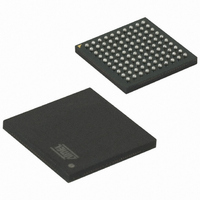
ATMEGA2560R231-AU Atmel, ATMEGA2560R231-AU Datasheet - Page 218

ATMEGA2560R231-AU
Manufacturer Part Number
ATMEGA2560R231-AU
Description
BUNDLE ATMEGA2560/RF231 TQFP
Manufacturer
Atmel
Datasheet
1.ATMEGA640V-8CU.pdf
(444 pages)
Specifications of ATMEGA2560R231-AU
Frequency
2.4GHz
Modulation Or Protocol
802.15.4 Zigbee, 6LoWPAN, RF4CE, SP100, WirelessHART™, ISM
Data Interface
PCB, Surface Mount
Memory Size
256kB Flash, 4kB EEPROM, 8kB RAM
Antenna Connector
PCB, Surface Mount
Package / Case
100-TFBGA
Processor Series
ATMEGA256x
Core
AVR8
Data Bus Width
8 bit
Program Memory Type
Flash
Program Memory Size
256 KB
Data Ram Size
8 KB
Development Tools By Supplier
ATAVRRZ541, ATAVRRAVEN, ATAVRRZRAVEN
Lead Free Status / RoHS Status
Lead free / RoHS Compliant
Voltage - Supply
-
Power - Output
-
Operating Temperature
-
Applications
-
Sensitivity
-
Data Rate - Maximum
-
Current - Transmitting
-
Current - Receiving
-
Lead Free Status / Rohs Status
Details
- Current page: 218 of 444
- Download datasheet (10Mb)
21.6.6
21.6.7
21.7
21.7.1
2549M–AVR–09/10
Asynchronous Data Reception
Disabling the Receiver
Flushing the Receive Buffer
Asynchronous Clock Recovery
The UPEn bit is set if the next character that can be read from the receive buffer had a Parity
Error when received and the Parity Checking was enabled at that point (UPMn1 = 1). This bit is
valid until the receive buffer (UDRn) is read.
In contrast to the Transmitter, disabling of the Receiver will be immediate. Data from ongoing
receptions will therefore be lost. When disabled (that is, the RXENn is set to zero) the Receiver
will no longer override the normal function of the RxDn port pin. The Receiver buffer FIFO will be
flushed when the Receiver is disabled. Remaining data in the buffer will be lost.
The receiver buffer FIFO will be flushed when the Receiver is disabled, that is, the buffer will be
emptied of its contents. Unread data will be lost. If the buffer has to be flushed during normal
operation, due to for instance an error condition, read the UDRn I/O location until the RXCn Flag
is cleared. The following code example shows how to flush the receive buffer.
Note:
The USART includes a clock recovery and a data recovery unit for handling asynchronous data
reception. The clock recovery logic is used for synchronizing the internally generated baud rate
clock to the incoming asynchronous serial frames at the RxDn pin. The data recovery logic sam-
ples and low pass filters each incoming bit, thereby improving the noise immunity of the
Receiver. The asynchronous reception operational range depends on the accuracy of the inter-
nal baud rate clock, the rate of the incoming frames, and the frame size in number of bits.
The clock recovery logic synchronizes internal clock to the incoming serial frames.
on page 219
rate is 16 times the baud rate for Normal mode, and eight times the baud rate for Double Speed
mode. The horizontal arrows illustrate the synchronization variation due to the sampling pro-
cess. Note the larger time variation when using the Double Speed mode (U2Xn = 1) of
operation. Samples denoted zero are samples done when the RxDn line is idle (that is, no com-
munication activity).
Assembly Code Example
C Code Example
USART_Flush:
void USART_Flush( void )
{
}
sbis UCSRnA, RXCn
ret
in
rjmp USART_Flush
unsigned char dummy;
while ( UCSRnA & (1<<RXCn) ) dummy = UDRn;
1. See “About Code Examples” on page 11.
illustrates the sampling process of the start bit of an incoming frame. The sample
r16, UDRn
(1)
(1)
ATmega640/1280/1281/2560/2561
Figure 21-5
218
Related parts for ATMEGA2560R231-AU
Image
Part Number
Description
Manufacturer
Datasheet
Request
R

Part Number:
Description:
Manufacturer:
ATMEL Corporation
Datasheet:

Part Number:
Description:
IC AVR MCU 256K 16MHZ 100TQFP
Manufacturer:
Atmel
Datasheet:

Part Number:
Description:
MCU AVR 256K FLASH 16MHZ 100TQFP
Manufacturer:
Atmel
Datasheet:

Part Number:
Description:
MCU AVR 256K FLASH 16MHZ 100CBGA
Manufacturer:
Atmel
Datasheet:

Part Number:
Description:
IC MCU AVR 256K FLASH 100-CBGA
Manufacturer:
Atmel
Datasheet:

Part Number:
Description:
IC AVR MCU 256K 16MHZ 100TQFP
Manufacturer:
Atmel
Datasheet:

Part Number:
Description:
DEV KIT FOR AVR/AVR32
Manufacturer:
Atmel
Datasheet:

Part Number:
Description:
INTERVAL AND WIPE/WASH WIPER CONTROL IC WITH DELAY
Manufacturer:
ATMEL Corporation
Datasheet:

Part Number:
Description:
Low-Voltage Voice-Switched IC for Hands-Free Operation
Manufacturer:
ATMEL Corporation
Datasheet:

Part Number:
Description:
MONOLITHIC INTEGRATED FEATUREPHONE CIRCUIT
Manufacturer:
ATMEL Corporation
Datasheet:


