APT75GP120J Microsemi Power Products Group, APT75GP120J Datasheet - Page 2
APT75GP120J
Manufacturer Part Number
APT75GP120J
Description
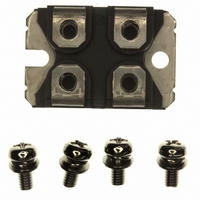
IGBT 1200V 128A 543W SOT227
Manufacturer
Microsemi Power Products Group
Series
POWER MOS 7®r
Datasheet
1.APT75GP120J.pdf
(6 pages)
Specifications of APT75GP120J
Igbt Type
PT
Configuration
Single
Voltage - Collector Emitter Breakdown (max)
1200V
Vce(on) (max) @ Vge, Ic
3.9V @ 15V, 75A
Current - Collector (ic) (max)
128A
Current - Collector Cutoff (max)
1mA
Input Capacitance (cies) @ Vce
7.04nF @ 25V
Power - Max
543W
Input
Standard
Ntc Thermistor
No
Mounting Type
Chassis Mount
Package / Case
ISOTOP
Lead Free Status / RoHS Status
Lead free / RoHS Compliant
Other names
APT75GP120JMI
APT75GP120JMI
APT75GP120JMI
Available stocks
Company
Part Number
Manufacturer
Quantity
Price
Company:

Part Number:
APT75GP120J
Manufacturer:
Microsemi Power Products Group
Quantity:
135
Company:
Part Number:
APT75GP120JDF3
Manufacturer:
TI/NSC
Quantity:
20 000
Company:
Part Number:
APT75GP120JDQ3
Manufacturer:
MICRON
Quantity:
101


DYNAMIC CHARACTERISTICS
THERMAL AND MECHANICAL CHARACTERISTICS
1 Repetitive Rating: Pulse width limited by maximum junction temperature.
2 For Combi devices, I
3 See MIL-STD-750 Method 3471.
4 E
5 E
6 E
Symbol
Symbol
RBSOA
V
R
R
C
t
t
t
t
E
E
E
E
adding to the IGBT turn-on loss. (See Figure 24.)
loss. A Combi device is used for the clamping diode as shown in the E
APT Reserves the right to change, without notice, the specifications and information contained herein.
C
C
Q
Q
d(on)
d(off)
E
d(on)
d(off)
E
W
Q
GEP
on1
on2
off
on1
on2
on1
on2
oes
t
t
t
t
res
ies
off
off
ge
gc
r
f
r
f
g
JC
JC
T
is the clamped inductive turn-off energy measured in accordance with JEDEC standard JESD24-1. (See Figures 21, 23.)
is the clamped inductive turn-on-energy of the IGBT only, without the effect of a commutating diode reverse recovery current
is the clamped inductive turn-on energy that includes a commutating diode reverse recovery current in the IGBT turn-on switching
Characteristic
Input Capacitance
Output Capacitance
Reverse Transfer Capacitance
Gate-to-Emitter Plateau Voltage
Total Gate Charge
Gate-Emitter Charge
Gate-Collector ("Miller ") Charge
Reverse Bias Safe Operating Area
Turn-on Delay Time
Current Rise Time
Turn-off Delay Time
Current Fall Time
Turn-on Switching Energy
Turn-on Switching Energy (Diode)
Turn-off Switching Energy
Turn-on Delay Time
Current Rise Time
Turn-off Delay Time
Current Fall Time
Turn-on Switching Energy
Turn-on Switching Energy (Diode)
Turn-off Switching Energy
Characteristic
Junction to Case (IGBT)
Junction to Case (DIODE)
Package Weight
ces
includes both IGBT and FRED leakages
3
6
4
4
6
5
5
Inductive Switching (125°C)
15V, L = 100µH,V
Inductive Switching (25°C)
T
J
= 150°C, R
V
GE
Test Conditions
Capacitance
Gate Charge
= 0V, V
T
V
V
V
T
on2
V
V
V
f = 1 MHz
J
CC
CC
CE
I
I
R
I
R
J
GE
GE
GE
C
C
C
= +125°C
= +25°C
G
G
test circuit. (See Figures 21, 22.)
= 75A
= 75A
= 75A
= 600V
= 600V
= 600V
= 15V
= 15V
= 15V
= 5
= 5
G
CE
= 5
CE
= 25V
= 960V
V
GE
=
MIN
300
MIN
7035
1620
4100
2500
1620
5850
4820
TYP
TYP
460
320
140
163
244
115
7.5
80
50
20
40
56
20
40
APT75GP120J
MAX
MAX
29.2
N/A
.23
UNIT
°C/W
UNIT
gm
pF
nC
ns
µ
ns
µ
V
A
J
J
Related parts for APT75GP120J
Image
Part Number
Description
Manufacturer
Datasheet
Request
R

Part Number:
Description:
IGBT 600V 100A 463W TO247
Manufacturer:
Microsemi Power Products Group
Datasheet:

Part Number:
Description:
IGBT 600V 198A 833W TO264
Manufacturer:
Microsemi Power Products Group
Datasheet:
Part Number:
Description:
IGBT 600V 41A 187W TO247
Manufacturer:
Microsemi Power Products Group
Datasheet:
Part Number:
Description:
MOSFET N-CH 600V 23A TO-247
Manufacturer:
Microsemi Power Products Group
Datasheet:

Part Number:
Description:
MOSFET N-CH 500V 17A TO-220
Manufacturer:
Microsemi Power Products Group
Datasheet:
Part Number:
Description:
MOSFET N-CH 1200V 3.5A TO-220
Manufacturer:
Microsemi Power Products Group
Datasheet:
Part Number:
Description:
MOSFET N-CH 500V 22A TO-247
Manufacturer:
Microsemi Power Products Group
Datasheet:
Part Number:
Description:
MOSFET N-CH 100V 75A TO-247
Manufacturer:
Microsemi Power Products Group
Datasheet:
Part Number:
Description:
MOSFET N-CH 200V 56A TO-247
Manufacturer:
Microsemi Power Products Group
Datasheet:
Part Number:
Description:
MOSFET N-CH 500V 27A TO-247
Manufacturer:
Microsemi Power Products Group
Datasheet:
Part Number:
Description:
MOSFET N-CH 300V 40A TO-247
Manufacturer:
Microsemi Power Products Group
Datasheet:
Part Number:
Description:
MOSFET N-CH 200V 59A TO-247
Manufacturer:
Microsemi Power Products Group
Datasheet:
Part Number:
Description:
MOSFET N-CH 500V 26A TO-247
Manufacturer:
Microsemi Power Products Group
Datasheet:
Part Number:
Description:
MOSFET N-CH 300V 40A TO-247
Manufacturer:
Microsemi Power Products Group
Datasheet:
Part Number:
Description:
MOSFET N-CH 200V 65A TO-247
Manufacturer:
Microsemi Power Products Group
Datasheet: