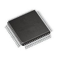
ATMEGA64A-MNR Atmel, ATMEGA64A-MNR Datasheet - Page 84

ATMEGA64A-MNR
Manufacturer Part Number
ATMEGA64A-MNR
Description
IC MCU AVR 64K FLASH 8QFN
Manufacturer
Atmel
Series
AVR® ATmegar
Datasheet
1.ATMEGA64A-AU.pdf
(392 pages)
Specifications of ATMEGA64A-MNR
Core Processor
AVR
Core Size
8-Bit
Speed
16MHz
Connectivity
I²C, SPI, UART/USART
Peripherals
Brown-out Detect/Reset, POR, PWM, WDT
Number Of I /o
53
Program Memory Size
64KB (32K x 16)
Program Memory Type
FLASH
Eeprom Size
2K x 8
Ram Size
4K x 8
Voltage - Supply (vcc/vdd)
2.7 V ~ 5.5 V
Data Converters
A/D 8x10b
Oscillator Type
Internal
Operating Temperature
-40°C ~ 85°C
Package / Case
*
Core
AVR8
Data Bus Width
8 bit
Data Ram Size
2 KB
Interface Type
SPI, UART, I2C
Maximum Clock Frequency
16 MHz
Number Of Programmable I/os
53
Operating Supply Voltage
2.7 V to 5.5 V
Maximum Operating Temperature
+ 105 C
Mounting Style
SMD/SMT
Operating Temperature Range
- 40 C to + 85 C
Processor To Be Evaluated
ATMEGA64A
Lead Free Status / RoHS Status
Lead free / RoHS Compliant
- Current page: 84 of 392
- Download datasheet (8Mb)
8160C–AVR–07/09
• AIN0/XCK0 – Port E, Bit 2
AIN0 – Analog Comparator Positive input. This pin is directly connected to the positive input of
the Analog Comparator.
XCK0, USART0 External Clock. The Data Direction Register (DDE2) controls whether the clock
is output (DDE2 set) or input (DDE2 cleared). The XCK0 pin is active only when the USART0
operates in synchronous mode.
• PDO/TXD0 – Port E, Bit 1
PDO, SPI Serial Programming Data output. During Serial Program Downloading, this pin is used
as data output line for the ATmega64A.
TXD0, UART0 Transmit Pin.
• PDI/RXD0 – Port E, Bit 0
PDI, SPI Serial Programming Data input. During serial program downloading, this pin is used as
data input line for the ATmega64A.
RXD0, USART0 Receive pin. Receive Data (Data Input pin for the USART0). When the
USART0 Receiver is enabled this pin is configured as an input regardless of the value of
DDRE0. When the USART0 forces this pin to be an input, a logical one in PORTE0 will turn on
the internal pull-up.
Table 13-16
shown in
Table 13-16. Overriding Signals for Alternate Functions PE7:PE4
Signal
Name
PUOE
PUOV
DDOE
DDOV
PVOE
PVOV
DIEOE
DIEOV
DI
AIO
Figure 13-5 on page
PE7/INT7/ICP3
0
0
0
0
0
1
INPUT
–
0
INT7 ENABLE
INT7 INPUT/ICP3
and
Table 13-17
relates the alternate functions of Port E to the overriding signals
73.
PE6/INT6/T3
0
0
0
0
0
0
INT6 ENABLE
1
INT7 INPUT/T3
INPUT
–
PE5/INT5/OC3C
0
0
0
0
OC3C ENABLE
OC3C
INT5 ENABLE
1
INT5 INPUT
–
ATmega64A
PE4/INT4/OC3B
0
0
0
0
OC3B ENABLE
OC3B
INT4 ENABLE
1
INT4 INPUT
–
84
Related parts for ATMEGA64A-MNR
Image
Part Number
Description
Manufacturer
Datasheet
Request
R

Part Number:
Description:
Manufacturer:
Atmel Corporation
Datasheet:

Part Number:
Description:
Manufacturer:
ATMEL Corporation
Datasheet:

Part Number:
Description:
Manufacturer:
ATMEL Corporation
Datasheet:

Part Number:
Description:
IC AVR MCU 64K 16MHZ 5V 64TQFP
Manufacturer:
Atmel
Datasheet:

Part Number:
Description:
IC AVR MCU 64K 16MHZ 5V 64-QFN
Manufacturer:
Atmel
Datasheet:

Part Number:
Description:
IC AVR MCU 64K 16MHZ COM 64-TQFP
Manufacturer:
Atmel
Datasheet:

Part Number:
Description:
IC AVR MCU 64K 16MHZ IND 64-TQFP
Manufacturer:
Atmel
Datasheet:

Part Number:
Description:
IC AVR MCU 64K 16MHZ COM 64-QFN
Manufacturer:
Atmel
Datasheet:

Part Number:
Description:
MCU AVR 64KB FLASH 16MHZ 64TQFP
Manufacturer:
Atmel
Datasheet:

Part Number:
Description:
MCU AVR 64KB FLASH 16MHZ 64QFN
Manufacturer:
Atmel
Datasheet:

Part Number:
Description:
IC AVR MCU 64K 16MHZ IND 64-QFN
Manufacturer:
Atmel
Datasheet:

Part Number:
Description:
IC MCU AVR 64K 5V 16MHZ 64-TQFP
Manufacturer:
Atmel
Datasheet:

Part Number:
Description:
IC MCU AVR 64K 5V 16MHZ 64-QFN
Manufacturer:
Atmel
Datasheet:

Part Number:
Description:
MCU 8-Bit ATmega AVR RISC 64KB Flash 5V 64-Pin TQFP T/R
Manufacturer:
Atmel
Datasheet:


