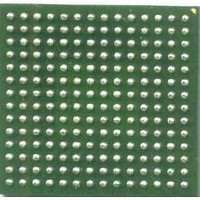
MCF53014CMJ240J Freescale Semiconductor, MCF53014CMJ240J Datasheet - Page 31

MCF53014CMJ240J
Manufacturer Part Number
MCF53014CMJ240J
Description
IC MCU 32BIT 128KB 256MAPBGA
Manufacturer
Freescale Semiconductor
Series
MCF5301xr
Datasheet
1.MCF53010CQT240.pdf
(62 pages)
Specifications of MCF53014CMJ240J
Core Processor
Coldfire V3
Core Size
32-Bit
Speed
240MHz
Connectivity
EBI/EMI, Ethernet, I²C, MMC, SPI, SSI, UART/USART, USB, USB OTG
Peripherals
DMA, PWM, WDT
Number Of I /o
83
Program Memory Size
16KB (16K x 8)
Program Memory Type
Cache
Ram Size
128K x 8
Voltage - Supply (vcc/vdd)
1.08 V ~ 3.6 V
Oscillator Type
Internal
Operating Temperature
-40°C ~ 85°C
Package / Case
256-LBGA
Processor Series
MCF5301x
Core
ColdFire V3
Data Bus Width
32 bit
Data Ram Size
16 bit
Interface Type
I2C, UART, DSPI
Maximum Clock Frequency
400 KHz, 20 MHz, 25 MHz
Number Of Timers
4
Operating Supply Voltage
- 0.5 V to + 2 V
Maximum Operating Temperature
+ 85 C
Mounting Style
SMD/SMT
3rd Party Development Tools
JLINK-CF-BDM26, EWCF
Development Tools By Supplier
M53015EVB, M53017KIT, M53017MOD
Minimum Operating Temperature
- 40 C
On-chip Adc
13 bit
On-chip Dac
16 bit
Lead Free Status / RoHS Status
Lead free / RoHS Compliant
Eeprom Size
-
Data Converters
-
Lead Free Status / Rohs Status
Details
Available stocks
Company
Part Number
Manufacturer
Quantity
Price
Company:
Part Number:
MCF53014CMJ240J
Manufacturer:
Freescale Semiconductor
Quantity:
10 000
8
9
Freescale Semiconductor
Data input skew is derived from each DQS clock edge. It begins with a DQS transition and ends when the last data line
becomes valid. This input skew must include DDR memory output skew and system level board skew (due to routing or other
factors).
Data input hold is derived from each DQS clock edge. It begins with a DQS transition and ends when the first data line becomes
invalid.
SD_DQS3/SD_DQS2
SD_RAS, SD_CAS
SD_CSn,SD_WE,
D[31:24]/D[23:16]
SD_CLK
SD_CLK
DM3/DM2
SD_CLK
SD_CLK
A[13:0]
DD4
Figure 15. SD_CLK and SD_CLK Crossover Timing
Preliminary—Subject to Change Without Notice
ROW
CMD
DD1
Figure 16. DDR Write Timing
MCF5301x Data Sheet, Rev. 5
DD5
COL
DD6
WD1 WD2 WD3 WD4
DD2
DD3
Preliminary Electrical Characteristics
DD7
DD7
DD8
DD8
V
V
V
IX
MP
IX
V
ID
31


