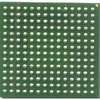
MCF53014CMJ240J Freescale Semiconductor, MCF53014CMJ240J Datasheet - Page 9

MCF53014CMJ240J
Manufacturer Part Number
MCF53014CMJ240J
Description
IC MCU 32BIT 128KB 256MAPBGA
Manufacturer
Freescale Semiconductor
Series
MCF5301xr
Datasheet
1.MCF53010CQT240.pdf
(62 pages)
Specifications of MCF53014CMJ240J
Core Processor
Coldfire V3
Core Size
32-Bit
Speed
240MHz
Connectivity
EBI/EMI, Ethernet, I²C, MMC, SPI, SSI, UART/USART, USB, USB OTG
Peripherals
DMA, PWM, WDT
Number Of I /o
83
Program Memory Size
16KB (16K x 8)
Program Memory Type
Cache
Ram Size
128K x 8
Voltage - Supply (vcc/vdd)
1.08 V ~ 3.6 V
Oscillator Type
Internal
Operating Temperature
-40°C ~ 85°C
Package / Case
256-LBGA
Processor Series
MCF5301x
Core
ColdFire V3
Data Bus Width
32 bit
Data Ram Size
16 bit
Interface Type
I2C, UART, DSPI
Maximum Clock Frequency
400 KHz, 20 MHz, 25 MHz
Number Of Timers
4
Operating Supply Voltage
- 0.5 V to + 2 V
Maximum Operating Temperature
+ 85 C
Mounting Style
SMD/SMT
3rd Party Development Tools
JLINK-CF-BDM26, EWCF
Development Tools By Supplier
M53015EVB, M53017KIT, M53017MOD
Minimum Operating Temperature
- 40 C
On-chip Adc
13 bit
On-chip Dac
16 bit
Lead Free Status / RoHS Status
Lead free / RoHS Compliant
Eeprom Size
-
Data Converters
-
Lead Free Status / Rohs Status
Details
Available stocks
Company
Part Number
Manufacturer
Quantity
Price
Company:
Part Number:
MCF53014CMJ240J
Manufacturer:
Freescale Semiconductor
Quantity:
10 000
Executing
Run
Wait
Doze
Stop(0)
Stop(1)
Stop(2)
Stop(3)
Stop Mode
4
4.1
The following table lists all the MCF5301x pins grouped by function. The “Dir” column is the direction for the primary function
of the pin only. Refer to
For a more detailed discussion of the MCF3xxx signals, consult the MCF5301x Reference Manual (MCF53017RM).
Freescale Semiconductor
Pin Assignments and Reset States
Signal Multiplexing
480VCO, 240MHz
In this table and throughout this document a single signal within a group is designated
without square brackets (i.e., FB_A23), while designations for multiple signals within a
group use brackets (i.e., FB_A[23:21]) and is meant to include all signals within the two
bracketed numbers when these numbers are separated by a colon.
The primary functionality of a pin is not necessarily its default functionality. Most pins that
are muxed with GPIO will default to their GPIO functionality. See
exceptions.
16.28mA
16.19mA
55.3mA
39.5mA
8.41mA
8.13mA
1.83mA
0.65mA
Table 4. Current Measurementas at Different VCO vs. Core Frequencies
core
Section 4.2, “Pinout—208
Table 5. Special-Case Default Signal Functionality
Preliminary—Subject to Change Without Notice
240VCO, 120MHz
FB_BE/BWE[3:0]
28.36mA
20.3mA
8.53mA
8.53mA
4.60mA
4.48mA
1.86mA
0.66mA
FB_CS[3:0]
core
FB_R/W
FB_OE
FB_TS
FB_TA
MCF5301x Data Sheet, Rev. 5
Pin
LQFP,”
NOTE
NOTE
and
480VCO, 120MHz
FB_BE/BWE[3:0]
Section 4.3, “Pinout–256
Default Signal
30.00mA
22.02mA
10.23mA
10.18mA
6.29mA
6.15mA
1.87mA
0.67mA
FB_CS[3:0]
core
FB_R/W
FB_OE
FB_TS
FB_TA
480VCO, 48MHz
Table 5
10.29mA
Pin Assignments and Reset States
13.6mA
5.53mA
5.55mA
3.90mA
3.88mA
1.82mA
0.67mA
MAPBGA,”
core
for a list of the
for package diagrams.
Limp Mode, 20HMHz
5.90mA
4.42mA
2.43mA
2.41mA
1.78mA
1.77mA
1.76mA
0.65mA
crystal
9


