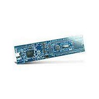
OM11049,598 NXP Semiconductors, OM11049,598 Datasheet - Page 13

OM11049,598
Manufacturer Part Number
OM11049,598
Description
MCU, MPU & DSP Development Tools LPC1114 Demo Boards Cortex M0
Manufacturer
NXP Semiconductors
Datasheet
1.OM11049598.pdf
(66 pages)
Specifications of OM11049,598
Processor To Be Evaluated
LPC1114
Processor Series
LPC11xx
Interface Type
I2C, SPI
Maximum Operating Temperature
+ 85 C
Minimum Operating Temperature
- 40 C
Operating Supply Voltage
3.3 V
Tool Type
Demonstration Board
Core Architecture
ARM
Cpu Core
ARM Cortex M0
Data Bus Width
32 bit
Lead Free Status / RoHS Status
Lead free / RoHS Compliant
NXP Semiconductors
Table 4.
LPC1111_12_13_14
Product data sheet
Symbol
PIO0_0 to PIO0_11
RESET/PIO0_0
PIO0_1/CLKOUT/
CT32B0_MAT2
PIO0_2/SSEL0/
CT16B0_CAP0
PIO0_3
PIO0_4/SCL
PIO0_5/SDA
PIO0_6/SCK0
PIO0_7/CTS
PIO0_8/MISO0/
CT16B0_MAT0
PIO0_9/MOSI0/
CT16B0_MAT1
SWCLK/PIO0_10/
SCK0/CT16B0_MAT2
LPC1114 pin description table (PLCC44 package)
Pin
7
8
14
18
19
20
26
27
31
32
33
[2]
[3]
[3]
[3]
[4]
[4]
[3]
[3]
[3]
[3]
[3]
Start
logic
input
yes
yes
yes
yes
yes
yes
yes
yes
yes
yes
yes
Type Reset
I/O
I
I/O
I/O
O
O
I/O
I/O
I
I/O
I/O
I/O
I/O
I/O
I/O
I/O
I/O
I
I/O
I/O
O
I/O
I/O
O
I
I/O
I/O
O
All information provided in this document is subject to legal disclaimers.
state
[1]
I; PU
-
I; PU
-
-
I; PU
-
-
I; PU
I; PU
-
I; PU
-
I; PU
-
I; PU
-
I; PU
-
-
I; PU
-
-
I; PU
-
-
-
Rev. 4 — 10 February 2011
Description
Port 0 — Port 0 is a 12-bit I/O port with individual direction and
function controls for each bit. The operation of port 0 pins depends
on the function selected through the IOCONFIG register block.
RESET — External reset input with 20 ns glitch filter. A LOW-going
pulse as short as 50 ns on this pin resets the device, causing I/O
ports and peripherals to take on their default states and processor
execution to begin at address 0.
PIO0_0 — General purpose digital input/output pin with 10 ns glitch
filter.
PIO0_1 — General purpose digital input/output pin. A LOW level on
this pin during reset starts the ISP command handler.
CLKOUT — Clockout pin.
CT32B0_MAT2 — Match output 2 for 32-bit timer 0.
PIO0_2 — General purpose digital input/output pin.
SSEL0 — Slave Select for SPI0.
CT16B0_CAP0 — Capture input 0 for 16-bit timer 0.
PIO0_3 — General purpose digital input/output pin.
PIO0_4 — General purpose digital input/output pin (open-drain).
SCL — I
only if I
register.
PIO0_5 — General purpose digital input/output pin (open-drain).
SDA — I
if I
PIO0_6 — General purpose digital input/output pin.
SCK0 — Serial clock for SPI0.
PIO0_7 — General purpose digital input/output pin (high-current
output driver).
CTS — Clear To Send input for UART.
PIO0_8 — General purpose digital input/output pin.
MISO0 — Master In Slave Out for SPI0.
CT16B0_MAT0 — Match output 0 for 16-bit timer 0.
PIO0_9 — General purpose digital input/output pin.
MOSI0 — Master Out Slave In for SPI0.
CT16B0_MAT1 — Match output 1 for 16-bit timer 0.
SWCLK — Serial wire clock.
PIO0_10 — General purpose digital input/output pin.
SCK0 — Serial clock for SPI0.
CT16B0_MAT2 — Match output 2 for 16-bit timer 0.
2
C Fast-mode Plus is selected in the I/O configuration register.
2
C Fast-mode Plus is selected in the I/O configuration
2
2
C-bus, open-drain clock input/output. High-current sink
C-bus, open-drain data input/output. High-current sink only
32-bit ARM Cortex-M0 microcontroller
LPC1111/12/13/14
© NXP B.V. 2011. All rights reserved.
13 of 66


