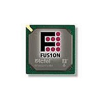
AFS250-PQG208 Actel, AFS250-PQG208 Datasheet - Page 167

AFS250-PQG208
Manufacturer Part Number
AFS250-PQG208
Description
FPGA - Field Programmable Gate Array 250K System Gates
Manufacturer
Actel
Datasheet
1.AFS600-PQG208.pdf
(330 pages)
Specifications of AFS250-PQG208
Processor Series
AFS250
Core
IP Core
Maximum Operating Frequency
1098.9 MHz
Number Of Programmable I/os
93
Data Ram Size
36864
Supply Voltage (max)
1.575 V
Maximum Operating Temperature
+ 70 C
Minimum Operating Temperature
0 C
Development Tools By Supplier
AFS-Eval-Kit, AFS-BRD600, FlashPro 3, FlashPro Lite, Silicon-Explorer II, Silicon-Sculptor 3, SI-EX-TCA
Mounting Style
SMD/SMT
Supply Voltage (min)
1.425 V
Number Of Gates
250 K
Package / Case
PQFP-208
Lead Free Status / RoHS Status
Lead free / RoHS Compliant
Available stocks
Company
Part Number
Manufacturer
Quantity
Price
Company:
Part Number:
AFS250-PQG208
Manufacturer:
NXP
Quantity:
8 000
Company:
Part Number:
AFS250-PQG208I
Manufacturer:
MPS
Quantity:
12 000
Company:
Part Number:
AFS250-PQG208I
Manufacturer:
Microsemi SoC
Quantity:
10 000
Part Number:
AFS250-PQG208I
Manufacturer:
MICROSEMI/美高森美
Quantity:
20 000
- Current page: 167 of 330
- Download datasheet (13Mb)
Selectable Skew between Output Buffer Enable/Disable Time
The configurable skew block is used to delay the output buffer assertion (enable) without affecting
deassertion (disable) time.
Figure 2-105 • Block Diagram of Output Enable Path
Figure 2-106 • Timing Diagram (option1: bypasses skew circuit)
Figure 2-107 • Timing Diagram (option 2: enables skew circuit)
(from FPGA core)
ENABLE (OUT)
Output Enable
ENABLE (OUT)
ENABLE (IN)
ENABLE (IN)
ENABLE (IN)
Less than
0.1 ns
(typical)
1.2 ns
Skew Circuit
R e v i s i o n 1
Skew Select
MUX
Less than
0.1 ns
Less than
0.1 ns
Actel Fusion Family of Mixed Signal FPGAs
ENABLE (OUT)
I/O Output
Buffers
2- 151
Related parts for AFS250-PQG208
Image
Part Number
Description
Manufacturer
Datasheet
Request
R

Part Number:
Description:
FPGA - Field Programmable Gate Array 250K System Gates
Manufacturer:
Actel
Datasheet:

Part Number:
Description:
FPGA 256/I�/Fusion Voltage: 1.5, 1.8, 2.5, 3.3 Mixed Voltage
Manufacturer:
Actel
Datasheet:

Part Number:
Description:
MCU, MPU & DSP Development Tools Silicon Sculptor Programming Mod
Manufacturer:
Actel

Part Number:
Description:
MCU, MPU & DSP Development Tools InSystem Programming ProASICPLUS Devices
Manufacturer:
Actel

Part Number:
Description:
Programming Socket Adapters & Emulators PQ160 Module
Manufacturer:
Actel

Part Number:
Description:
Programming Socket Adapters & Emulators Axcelerator Adap Module Kit
Manufacturer:
Actel

Part Number:
Description:
Programming Socket Adapters & Emulators Evaluation
Manufacturer:
Actel

Part Number:
Description:
Programming Socket Adapters & Emulators AFDX Solutions
Manufacturer:
Actel

Part Number:
Description:
Programming Socket Adapters & Emulators SILICON SCULPTOR ADAPTER MODULE
Manufacturer:
Actel
Datasheet:

Part Number:
Description:
Programming Socket Adapters & Emulators Axcelerator Adap Module Kit
Manufacturer:
Actel

Part Number:
Description:
Programming Socket Adapters & Emulators Evaluation
Manufacturer:
Actel

Part Number:
Description:
Programming Socket Adapters & Emulators Silicon Sculptor Software
Manufacturer:
Actel

Part Number:
Description:
Programming Socket Adapters & Emulators InSystem Programming ProASICPLUS Devices
Manufacturer:
Actel


