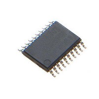
FMS6346EMTC20X Fairchild Semiconductor, FMS6346EMTC20X Datasheet - Page 11

FMS6346EMTC20X
Manufacturer Part Number
FMS6346EMTC20X
Description
IC DVR VFD SD/HD 6CH 20-TSSOP
Manufacturer
Fairchild Semiconductor
Type
Filter Driverr
Datasheet
1.FMS6346EMTC20X.pdf
(14 pages)
Specifications of FMS6346EMTC20X
Applications
Set-Top Boxes, Video Players
Mounting Type
Surface Mount
Package / Case
20-TSSOP (0.173", 4.40mm Width)
Driver Type
Video Filter Driver
Operating Supply Voltage
6 V
Maximum Operating Temperature
+ 85 C
Mounting Style
SMD/SMT
Maximum Output Current
50 mA
Maximum Power Dissipation
84 ns
Minimum Operating Temperature
- 40 C
Supply Current
50 mA
Lead Free Status / RoHS Status
Lead free / RoHS Compliant
Available stocks
Company
Part Number
Manufacturer
Quantity
Price
Part Number:
FMS6346EMTC20X
Manufacturer:
FAIRCHILD/仙童
Quantity:
20 000
© 2010 Fairchild Semiconductor Corporation
FMS6346E • Rev.2.0.10
The same method can be used to bias the clamp
signals.
External video
source must
be AC coupled
Figure 15. Biased SCART with DC-Coupled Outputs
The same circuits can be used with AC-coupled outputs
if desired, as shown in Figure 16.
Figure 18. Biased SCART with AC-Coupled Outputs
Note:
6.
External video
source must
be AC coupled.
Figure 16. DC-Coupled Inputs, AC-Coupled Outputs
Figure 17. Coupled Inputs, AC-Coupled Outputs
DVD or
DVD or
Output
Output
DAC
STB
SoC
DAC
STB
SoC
75W
The video tilt or line time distortion is dominated by
the AC-coupling capacitor. The value may need to
be increased beyond 220μF to obtain satisfactory
operation in some applications.
75Ω
500mV +/-350mV
0V - 1.4V
0.1µF
0.1μF
500mV +/-350mV
7.5MW
0.1μF
7.5MΩ
0V - 1.4V
Inactive
Clamp
LCVF
Clamp
Active
LCVF
Clamp
Active
LCVF
LCVF
Input
Bias
75
75W
75Ω
220µF
75Ω
220µF
220μF
11
Power Dissipation
The FMS6346E output drive configuration must be
considered when calculating overall power dissipation.
Care must be taken not to exceed the maximum die
junction temperature. The following example can be
used to calculate the power dissipation and internal
temperature rise:
Board layout affects thermal characteristics. Refer to
the Layout Considerations section for more information.
Output Considerations
The FMS6346E outputs are DC offset from the input by
150mV; therefore V
is required to obtain optimal performance from the
output driver and is held at the minimum value to
decrease the standing DC current into the load. Since
the FMS6346E has a 2x (6dB) gain, the output is
typically connected via a 75Ω series back-matching
resistor followed by the 75Ω video cable. Due to the
inherent divide by two of this configuration, the blanking
level at the load of the video signal is always less then
1V. When AC-coupling the output, ensure that the
coupling capacitor passes the lowest frequency content
in the video signal and that line time distortion (video
tilt) is kept as low as possible.
The selection of the coupling capacitor is a function of
the subsequent circuit input impedance and the leakage
current of the input driven. To obtain the highest quality
output video signal, the series termination resistor must
be placed as close to the device output pin as possible.
This greatly reduces the parasitic capacitance and
inductance effect on the output driver. The distance
from the device pin to the series termination resistor
should be no greater than 0.5 inches.
T
J
Figure 19. Distance from Device Pin to Series
= T
where P
P
where V
I
V
I
R
CH
CC
CHx
IN
L
A
= channel load resistance
= (I
= 50mA, V
= RMS value of input signal
+ P
= V
CC
d
d
O
S
• θ
/ 6) + (V
= P
• I
= 2V
JA
CH
CH1
S
IN
- (V
= 3.3V
OUT
+ P
+ 0.280V
O
Termination Resistor
O
/R
2
= 2•V
CH2
/R
L
)
L
)
+ P
IN
CHx
DC+150mV. This offset
and
www.fairchildsemi.com
(1)


