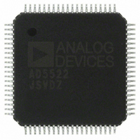
AD5522JSVDZ Analog Devices Inc, AD5522JSVDZ Datasheet - Page 21

AD5522JSVDZ
Manufacturer Part Number
AD5522JSVDZ
Description
IC, DAC, 16BIT, QFP-80
Manufacturer
Analog Devices Inc
Datasheet
1.AD5522JSVDZ.pdf
(64 pages)
Specifications of AD5522JSVDZ
Resolution (bits)
16bit
Input Channel Type
Serial
Supply Voltage Range - Digital
2.3V To 5.25V
Supply Current
36mA
Digital Ic Case Style
QFP
No. Of Pins
80
Data Interface
LVDS, Serial
Design Resources
Parametric Measurement Unit and Supporting Components for PAD Appls Using AD5522 and AD7685 (CN0104)
Lead Free Status / RoHS Status
Lead free / RoHS Compliant
Available stocks
Company
Part Number
Manufacturer
Quantity
Price
Company:
Part Number:
AD5522JSVDZ
Manufacturer:
WD
Quantity:
1 000
Company:
Part Number:
AD5522JSVDZ
Manufacturer:
Analog Devices Inc
Quantity:
10 000
Part Number:
AD5522JSVDZ
Manufacturer:
ADI/亚德诺
Quantity:
20 000
Pin No.
46
47
48
49
50
51
52
53
54
55
56
57
58
60
62
63
64
65
66
67
68
69
72
73
74
75
76
77
78
79
Mnemonic
CPOL2/CPO0
DVCC
LOAD
SDO
CPOH1/SDO
DGND
CPOL1/SYNC
SYNC
SDI
CPOH0/SDI
CPOL0/SCLK
SCLK
BUSY
EXTFOH2
CFF2
CCOMP2
EXTMEASIH2
EXTMEASIL2
FOH2
GUARD2
GUARDIN2/
DUTGND2
MEASVH2
MEASVH0
GUARDIN0/
DUTGND0
GUARD0
FOH0
EXTMEASIL0
EXTMEASIH0
CCOMP0
CFF0
Description
Comparator Output Low (Channel 2) for SPI Interface/Comparator Output Window (Channel 0) for LVDS
Interface.
Digital Supply Voltage.
Logic Input (Active Low). This pin synchronizes updates within one device or across a group of devices. If
synchronization is not required, LOAD can be tied low; in this case, DAC channels and PMU modes are updated
immediately after BUSY goes high. See the BUSY and LOAD Functions section for more information.
Serial Data Output for SPI or LVDS Interface. This pin can be used for data readback and diagnostic purposes.
Comparator Output High (Channel 1) for SPI Interface/Differential Serial Data Output (Complement) for LVDS
Interface.
Digital Ground Reference Point.
Comparator Output Low (Channel 1) for SPI Interface/Differential SYNC Input for LVDS Interface.
Active Low Frame Synchronization Input for SPI or LVDS Interface.
Serial Data Input for SPI or LVDS Interface.
Comparator Output High (Channel 0) for SPI Interface/Differential Serial Data Input (Complement) for LVDS
Interface.
Comparator Output Low (Channel 0) for SPI Interface/Differential Serial Clock Input (Complement) for LVDS
Interface.
Serial Clock Input, Active Falling Edge. Data is clocked into the shift register on the falling edge of SCLK. This
pin operates at clock speeds up to 50 MHz.
Digital Input/Open-Drain Output. This pin indicates the status of the interface. See the BUSY and LOAD
Functions section for more information.
Force Output for High Current Range (Channel 2). Use an external resistor at this pin for current ranges up to
±80 mA. For more information, see the Current Range Selection section.
External Capacitor for Channel 2. This pin optimizes the stability and settling time performance of the force
amplifier when in force voltage mode. See the Compensation Capacitors section.
Compensation Capacitor Input for Channel 2. See the Compensation Capacitors section.
Sense Input (High Sense) for High Current Range (Channel 2).
Sense Input (Low Sense) for High Current Range (Channel 2).
Force Output for Internal Current Ranges (Channel 2).
Guard Output Drive for Channel 2.
Guard Amplifier Input for Channel 2/DUTGND Input for Channel 2. This dual function pin is configured via the
serial interface. The default function at power-on is GUARDIN2. If this pin is configured as a DUTGND input for
the channel, the input to the guard amplifier is internally connected to MEASVH2. For more information, see
the Device Under Test Ground (DUTGND) section and the Guard Amplifier section.
DUT Voltage Sense Input (High Sense) for Channel 2.
DUT Voltage Sense Input (High Sense) for Channel 0.
Guard Amplifier Input for Channel 0/DUTGND Input for Channel 0. This dual function pin is configured via the
serial interface. The default function at power-on is GUARDIN0. If this pin is configured as a DUTGND input for
the channel, the input to the guard amplifier is internally connected to MEASVH0. For more information, see
the Device Under Test Ground (DUTGND) section and the Guard Amplifier section.
Guard Output Drive for Channel 0.
Force Output for Internal Current Ranges (Channel 0).
Sense Input (Low Sense) for High Current Range (Channel 0).
Sense Input (High Sense) for High Current Range (Channel 0).
Compensation Capacitor Input for Channel 0. See the Compensation Capacitors section.
External Capacitor for Channel 0. This pin optimizes the stability and settling time performance of the force
amplifier when in force voltage mode. See the Compensation Capacitors section.
Rev. D | Page 21 of 64
AD5522


