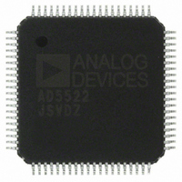
AD5522JSVDZ Analog Devices Inc, AD5522JSVDZ Datasheet - Page 58

AD5522JSVDZ
Manufacturer Part Number
AD5522JSVDZ
Description
IC, DAC, 16BIT, QFP-80
Manufacturer
Analog Devices Inc
Datasheet
1.AD5522JSVDZ.pdf
(64 pages)
Specifications of AD5522JSVDZ
Resolution (bits)
16bit
Input Channel Type
Serial
Supply Voltage Range - Digital
2.3V To 5.25V
Supply Current
36mA
Digital Ic Case Style
QFP
No. Of Pins
80
Data Interface
LVDS, Serial
Design Resources
Parametric Measurement Unit and Supporting Components for PAD Appls Using AD5522 and AD7685 (CN0104)
Lead Free Status / RoHS Status
Lead free / RoHS Compliant
Available stocks
Company
Part Number
Manufacturer
Quantity
Price
Company:
Part Number:
AD5522JSVDZ
Manufacturer:
WD
Quantity:
1 000
Company:
Part Number:
AD5522JSVDZ
Manufacturer:
Analog Devices Inc
Quantity:
10 000
Part Number:
AD5522JSVDZ
Manufacturer:
ADI/亚德诺
Quantity:
20 000
AD5522
APPLICATIONS INFORMATION
POWER-ON DEFAULT
The power-on default for all DAC channels is that the contents
of each M register are set to full scale (0xFFFF), and the contents
of each C register are set to midscale (0x8000). The contents of
the DAC X1 registers at power-on are listed in Table 36.
The power-on default for the alarm status register is 0xFFFFF0,
and the power-on default for the comparator status register is
0x400000. The power-on default values of the PMU register and
the system control register are shown in Table 37 and Table 38.
SETTING UP THE DEVICE ON POWER-ON
On power-on, default conditions are recalled from the power-
on reset register to ensure that each PMU and DAC channel is
powered up in a known condition. To operate the device, the
user must follow these steps:
1.
2.
3.
4.
Table 36. Default Contents of DAC Registers at Power-On
DAC Register
Offset DAC
FIN DAC
CLL DAC
CLH DAC
CPL DAC
CPH DAC
Configure the device by writing to the system control
register to set up different functions as required.
Calibrate the device to trim out errors, and load the
required calibration values to the gain (M) and offset (C)
registers. Load codes to each DAC input (X1) register.
When X1 values are loaded to the individual DACs, the
calibration engine calculates the appropriate X2 value and
stores it, ready for the PMU address to call it.
Load the required PMU channel with the required force
mode, current range, and so on. Loading the PMU channel
configures the switches around the force amplifier,
measure function, clamps, and comparators, and also acts
as a load signal for the DACs, loading the DAC register
with the appropriate stored X2 value.
Because the voltage and current ranges have individual
DAC registers associated with them, each PMU register
mode of operation calls a particular X2 register. Therefore,
only updates (that is, changes to the X1 register) to DACs
associated with the selected mode of operation are reflected
in the output of the PMU. If there is a change to the X1
value associated with a different PMU mode of operation,
this X1 value and its M and C coefficients are used to
calculate a corresponding X2 value, which is stored in the
correct X2 register, but this value is not loaded to the DAC.
Default Value
0xA492
0x8000
0x0000
0xFFFF
0x0000
0xFFFF
Rev. D | Page 58 of 64
Table 37. Power-On Default for System Control Register
Bit
21 (MSB)
20
19
18
17
16
15
14
13
12
11
10
9
8
7
6
5
4
3
2
1
0 (LSB)
Table 38. Power-On Default for PMU Register
Bit
21 (MSB)
20
19
18
17
16
15
14
13
12
11
10
9
8
7
6
5
4
3
2
1
0 (LSB)
Bit Name
CL3
CL2
CL1
CL0
CPOLH3
CPOLH2
CPOLH1
CPOLH0
CPBIASEN
DUTGND/CH
Guard ALM
Clamp ALM
INT10K
Guard EN
GAIN1
GAIN0
TMP enable
TMP1
TMP0
Latched
Unused data bit
Unused data bit
Bit Name
CH EN
FORCE1
FORCE0
Reserved
C2
C1
C0
MEAS1
MEAS0
FIN
SF0
SS0
CL
CPOLH
Compare V/I
LTMPALM
TMPALM
Unused data bit
Unused data bit
Unused data bit
Unused data bit
Unused data bit
Default Value
0
0
0
0
0
0
0
0
0
0
0
0
0
0
0
0
1
0
0
0
0
0
Default Value
0
0
0
0
0
1
1
1
1
0
0
0
0
0
0
1
1
0
0
0
0
0


