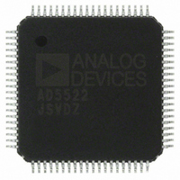
AD5522JSVDZ Analog Devices Inc, AD5522JSVDZ Datasheet - Page 39

AD5522JSVDZ
Manufacturer Part Number
AD5522JSVDZ
Description
IC, DAC, 16BIT, QFP-80
Manufacturer
Analog Devices Inc
Datasheet
1.AD5522JSVDZ.pdf
(64 pages)
Specifications of AD5522JSVDZ
Resolution (bits)
16bit
Input Channel Type
Serial
Supply Voltage Range - Digital
2.3V To 5.25V
Supply Current
36mA
Digital Ic Case Style
QFP
No. Of Pins
80
Data Interface
LVDS, Serial
Design Resources
Parametric Measurement Unit and Supporting Components for PAD Appls Using AD5522 and AD7685 (CN0104)
Lead Free Status / RoHS Status
Lead free / RoHS Compliant
Available stocks
Company
Part Number
Manufacturer
Quantity
Price
Company:
Part Number:
AD5522JSVDZ
Manufacturer:
WD
Quantity:
1 000
Company:
Part Number:
AD5522JSVDZ
Manufacturer:
Analog Devices Inc
Quantity:
10 000
Part Number:
AD5522JSVDZ
Manufacturer:
ADI/亚德诺
Quantity:
20 000
Calibration Example
Nominal offset coefficient = 32,768
Nominal gain coefficient = 65,535
For example, the gain error = 0.5%, and the offset error = 100 mV.
Gain error (0.5%) calibration:
Therefore, load Code 1111 1110 1011 0111 to the M register.
Offset error (100 mV) calibration:
Offset coefficient for 100 mV offset = 100/0.156 = 641 LSBs
Therefore, load Code 0111 1101 0111 1111 to the C register.
ADDITIONAL CALIBRATION
The techniques described in the Calibration section are usually
sufficient to reduce the zero-scale and gain errors. However,
there are limitations whereby the errors may not be sufficiently
reduced. For example, the offset (C) register can only be used to
reduce the offset caused by negative zero-scale error. A positive
offset cannot be reduced. Likewise, if the maximum voltage is
below the ideal value, that is, a negative gain error, the gain (M)
register cannot be used to increase the gain to compensate for
the error. These limitations can be overcome by increasing the
reference value.
SYSTEM LEVEL CALIBRATION
There are many ways to calibrate the device on power-on.
Following is an example of how to calibrate the FIN DAC of the
device without a DUT or DUT board connected.
65,535 × 0.995 = 65,207
LSB size = 10.25/65,535 = 156 μV
Rev. D | Page 39 of 64
The calibration procedure for the force and measure circuitry is
as follows:
1.
2.
3.
4.
5.
Similarly, calibrate the comparator and clamp DACs, and load
the appropriate gain and offset registers. Calibrating these
DACs requires some successive approximation to find where
the comparator trips or the clamps engage.
Calibrate the force voltage (2 points).
In FV mode, write zero scale to the FIN DAC. Connect
SYS_FORCE to FOHx and SYS_SENSE to MEASVHx,
and close the internal force/sense switch (SW7).
Using the system PMU, measure the error between the
voltage at FOHx/MEASVHx and the desired value.
Similarly, load full scale to the FIN DAC and measure the
error between the voltage at FOHx/MEASVHx and the
desired value. Calculate the M and C values. Load these
values to the appropriate M and C registers of the FIN DAC.
Calibrate the measure voltage (2 points).
Connect SYS_FORCE to FOHx and SYS_SENSE to
MEASVHx, and close the internal force/sense switch (SW7).
Force voltage on FOHx via SYS_FORCE and measure the
voltage at MEASOUTx. The difference is the error between
the actual forced voltage and the voltage at MEASOUTx.
Calibrate the force current (2 points).
In FI mode, write zero scale to the FIN DAC. Connect
SYS_FORCE to an external ammeter and to the FOHx pin.
Measure the error between the ammeter reading and the
MEASOUTx reading. Repeat this step with full scale
loaded to the FIN DAC. Calculate the M and C values.
Calibrate the measure current (2 points).
In FI mode, write zero scale to the FIN DAC. Connect
SYS_FORCE to an external ammeter and to the FOHx pin.
Measure the error between the ammeter reading and the
MEASOUTx reading. Repeat this step with full scale
loaded to the FIN DAC.
Repeat this procedure for all four channels.
AD5522


