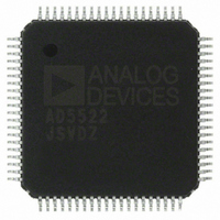
AD5522JSVDZ Analog Devices Inc, AD5522JSVDZ Datasheet - Page 42

AD5522JSVDZ
Manufacturer Part Number
AD5522JSVDZ
Description
IC, DAC, 16BIT, QFP-80
Manufacturer
Analog Devices Inc
Datasheet
1.AD5522JSVDZ.pdf
(64 pages)
Specifications of AD5522JSVDZ
Resolution (bits)
16bit
Input Channel Type
Serial
Supply Voltage Range - Digital
2.3V To 5.25V
Supply Current
36mA
Digital Ic Case Style
QFP
No. Of Pins
80
Data Interface
LVDS, Serial
Design Resources
Parametric Measurement Unit and Supporting Components for PAD Appls Using AD5522 and AD7685 (CN0104)
Lead Free Status / RoHS Status
Lead free / RoHS Compliant
Available stocks
Company
Part Number
Manufacturer
Quantity
Price
Company:
Part Number:
AD5522JSVDZ
Manufacturer:
WD
Quantity:
1 000
Company:
Part Number:
AD5522JSVDZ
Manufacturer:
Analog Devices Inc
Quantity:
10 000
Part Number:
AD5522JSVDZ
Manufacturer:
ADI/亚德诺
Quantity:
20 000
AD5522
SERIAL INTERFACE
The AD5522 provides two high speed serial interfaces: an SPI-
compatible interface operating at clock frequencies up to 50 MHz
and an EIA-644-compliant LVDS interface. To minimize both
the power consumption of the device and the on-chip digital
noise, the serial interface powers up fully only when the device
is being written to, that is, on the falling edge of SYNC .
SPI INTERFACE
The serial interface operates from a 2.3 V to 5.25 V DVCC supply
range. The SPI interface is selected when the SPI /LVDS pin is
held low. It is controlled by four pins, as described in
Table 15. Pins That Control the SPI Interface
Pin
SYNC
SDI
SCLK
SDO
LVDS INTERFACE
The LVDS interface uses the same input pins, with the same
designations, as the SPI interface. In addition, four other pins
are provided for the complementary signals needed for differ-
ential operation, as described in Table 16.
Table 16. Pins That Control the LVDS Interface
Pin
SYNC
SYNC
SDI
SDI
SCLK
SCLK
SDO
SDO
SERIAL INTERFACE WRITE MODE
The AD5522 allows writing of data via the serial interface to
every register directly accessible to the serial interface, that is,
all registers except the DAC registers.
The serial word is 29 bits long. The serial interface works with
both a continuous and a burst (gated) serial clock. Serial data
applied to SDI is clocked into the AD5522 by clock pulses
applied to SCLK. The first falling edge of SYNC starts the write
cycle. At least 29 falling clock edges must be applied to SCLK to
clock in 29 bits of data before SYNC is taken high again.
Description
Differential frame synchronization signal
Differential frame synchronization signal
(complement)
Differential serial data input
Differential serial data input (complement)
Differential serial clock input
Differential serial clock input (complement)
Differential serial data output for data readback
Differential serial data output for data readback
(complement)
Description
Frame synchronization input
Serial data input pin
Clocks data in and out of the device
Serial data output pin for data readback (weak
SDO output driver, may require reduction in SCLK
frequency to correctly read back, see Table 2)
Table 15
Rev. D | Page 42 of 64
.
The input register addressed is updated on the rising edge of
SYNC . For another serial transfer to take place, SYNC must be
taken low again.
The shift register can accept longer words (for example, 32-bit
words), framed by SYNC , but the data should always be in the
29
RESET FUNCTION
Bringing the level-sensitive RESET line low resets the contents
of all internal registers to their power-on reset state (see the
Power-On Default
600 μs.
RESET is brought high again and the initialization is complete.
While BUSY is low, all interfaces are disabled. When BUSY
returns high, normal operation resumes, and the status of the
RESET pin is ignored until it goes low again. The SDO output is
high impedance during a power-on reset or a RESET . A power-
on reset functions the same way as RESET .
BUSY AND LOAD FUNCTIONS
The BUSY pin is an open-drain output that indicates the status
of the AD5522 interface. When writing to any register, BUSY
goes low and stays low until the command completes.
A write operation to a DAC X1 register and some PMU register
bits (see Table 18) drives the BUSY signal low for longer than a
write M, C, or system control register. For DACs, the value of
the internal cached (X2) data is calculated and stored each time
that the user writes new data to the corresponding X1 register.
During the calculation and writing of X2, the BUSY output is
driven low. While BUSY is low, the user can continue writing
new data to the any register, but this write should not be
completed with SYNC going high until BUSY returns high (see
Figure 56
X2 values are stored and held until a PMU word is written that
calls the appropriate cached X2 register. Only then is a DAC
output updated.
The DAC outputs and PMU modes are updated by taking the
LOAD input low. If LOAD goes low while BUSY is active, the
LOAD event is stored and the DAC outputs or PMU modes are
updated immediately after BUSY goes high. A user can also hold
the LOAD input permanently low. In this case, the DAC outputs
or PMU modes are updated immediately after BUSY goes high.
The BUSY pin is bidirectional and has a 50 kΩ internal pull-up
resistor. When multiple AD5522 devices are used in one system,
the BUSY pins can be tied together. This is useful when it is
required that no DAC or PMU in any device be updated until
all others are ready to be updated. When each device finishes
updating its X2 registers, it releases the BUSY pin. If another
device has not finished updating its X2 registers, it holds BUSY
low, thus delaying the effect of LOAD going low.
th
LSB positions.
BUSY goes low for the duration, returning high when
and
Figure 57
section). This sequence takes approximately
).


