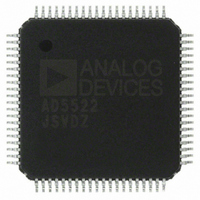
AD5522JSVDZ Analog Devices Inc, AD5522JSVDZ Datasheet - Page 51

AD5522JSVDZ
Manufacturer Part Number
AD5522JSVDZ
Description
IC, DAC, 16BIT, QFP-80
Manufacturer
Analog Devices Inc
Datasheet
1.AD5522JSVDZ.pdf
(64 pages)
Specifications of AD5522JSVDZ
Resolution (bits)
16bit
Input Channel Type
Serial
Supply Voltage Range - Digital
2.3V To 5.25V
Supply Current
36mA
Digital Ic Case Style
QFP
No. Of Pins
80
Data Interface
LVDS, Serial
Design Resources
Parametric Measurement Unit and Supporting Components for PAD Appls Using AD5522 and AD7685 (CN0104)
Lead Free Status / RoHS Status
Lead free / RoHS Compliant
Available stocks
Company
Part Number
Manufacturer
Quantity
Price
Company:
Part Number:
AD5522JSVDZ
Manufacturer:
WD
Quantity:
1 000
Company:
Part Number:
AD5522JSVDZ
Manufacturer:
Analog Devices Inc
Quantity:
10 000
Part Number:
AD5522JSVDZ
Manufacturer:
ADI/亚德诺
Quantity:
20 000
DAC Addressing
For the FIN and comparator (CPH and CPL) DACs, there is a
set of X1, M, and C registers for each current range, and one set
for the voltage range; for the clamp DACs (CLL and CLH),
there are only two sets of X1, M, and C registers.
When calibrating the device, the M and C registers allow volatile
storage of gain and offset coefficients. Calculation of the corres-
ponding DAC X2 register occurs only when the X1 data is loaded
(no internal calculation occurs on M or C updates).
There is one offset DAC for all four channels in the device that
is addressed using the PMUx bits. The offset DAC has only an
input register associated with it; no M or C registers are asso-
ciated with this DAC. When writing to the offset DAC, set the
Table 29. DAC Register Addressing
A5
0
0
0
0
0
0
0
0
0
0
0
1
A4
0
0
0
0
0
0
0
1
1
1
1
0
A3
0
1
1
1
1
1
1
0
0
1
1
0
A2
0
0
0
0
0
1
1
1
1
1
1
0
A1
0
0
0
1
1
0
0
0
0
0
0
0
A0
0
0
1
0
1
0
1
0
1
0
1
0
1
0
1
1
0
1
1
0
1
1
0
1
1
0
1
1
0
1
1
0
1
1
0
1
1
0
1
1
0
1
1
0
1
1
MODE1
Rev. D | Page 51 of 64
MODE0
1
1
0
1
1
0
1
1
0
1
1
0
1
1
0
1
1
0
1
1
0
1
1
0
1
1
0
1
1
0
1
1
0
1
MODE1 and MODE0 bits high to address the DAC input
register (X1).
The same address table is also used for readback of a particular
DAC address.
Note that CLL is clamp level low and CLH is clamp level high.
•
•
All codes not explicitly referenced Table 29 are reserved and
should not be used.
When forcing a voltage, the current clamps are engaged;
therefore, both the CLL current ranges register set and the
CLH current ranges register set are loaded to the clamp DACs.
When forcing a current, the voltage clamps are engaged;
therefore, both the CLL voltage range register set and the
CLH voltage range register set are loaded to the clamp DACs.
Register Set
N/A
±5 μA current range
±20 μA current range
±200 μA current range
±2 mA current range
±external current range
Voltage range
Current ranges
Voltage range
Current ranges
Voltage range
±5 μA current range
Addressed Register
Offset DAC X
FIN C
FIN X1
FIN C
FIN X1
FIN C
FIN X1
FIN C
FIN X1
FIN C
FIN X1
FIN C
FIN X1
CLL C
CLL X1
CLL C
CLL X1
CLH C
CLH X1
CLH C
CLH X1
CPL C
CPL X1
FIN M
FIN M
FIN M
FIN M
FIN M
FIN M
CLL M
CLL M
CLH M
CLH M
CPL M
1
2
AD5522


